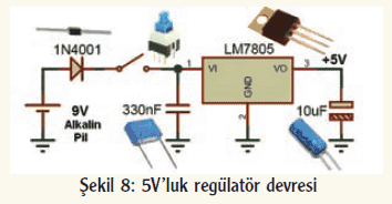
Differences between regulator circuits.

In summary, the first circuit can use the regulator circuit in the second circuit, but the capacitors are important.
  • #1
Zalajbeg
78
3
Hi everyone,

I want to understand how to decide what type of regulator I need to use in a circuit. I believe it will take much time to learn it totally but as a first step I am going to ask the differences between two regulator circuits.

A circuit and the 5V regulator it uses can be seen below:
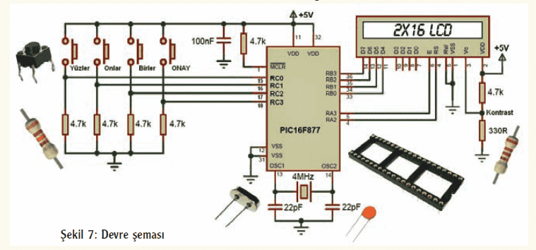
Circuit1.PNG


Regulator1.PNG


Another circuit uses a different regulator circuit:
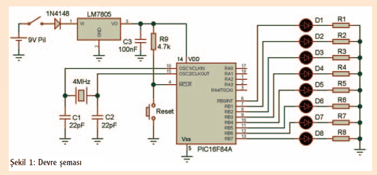
Circuit2.PNG


The question is that, cannot the first circuit use the regulator circuit in the second circuit (the one with no capacitor)? If not, why? As both of them supply a 5V output I cannot see the difference. Could you explain me why the capacitors are used?
 
Engineering news on Phys.org
  • #3
Bobbywhy said:
The best circuit for the LM7805 regulator in your examples is #2. It uses a capacitor on both the input to the regulator and on the output. Each is important: see this for explanation: http://www.learningaboutelectronics.com/Articles/How-do-you-connect-a-voltage-regulator-in-a-circuit
Good luck! İyi şanslar!

I have totally understood the logic. The capacitors are not much important for the first circuit as the noise will not affect much the LEDs. However in the second circuit the battery also supplies the input pin. As the input pin is sensible to 5V the noise is important. So it is important to use the capacitors when the regulator circuit supplies the input pins.

However I have one more question. The picture I sent shows the output capacitor as 10 μF and the page you sent shows it as 0.1 μF. I couldn't make sure how I must decide it. If I can use 0.1 μF, 0.33 μF or a similar magnitude it will be better to me. (As I can use ceramic ones I will make sure that someone will not link it wrong and will not cause a small explosion.).

Could you offer me a method to predict the value?

Çok teşekkürler!
 
  • #4
bir şey değil!

The capacitor at the output of the LM 7805 functions to protect the output voltage from changing during large transients of load current. It “smoothes” the output voltage.

You could easily test this by selecting a typical value, for instance, 1 or 10 microfarad. Then operate your circuit while monitoring the output voltage with your oscilloscope. Set the “vertical sensitivity” control higher and higher, looking for voltage dips (sags) when the circuit draws current. The larger the current spikes, the more capacitance is needed to avoid voltage drops. Think of it a mechanical shock absorber. If your load does not draw large transient currents, the output capacitor can be smaller.

Your English is excellent!
 
  • #5
Re your first figure: Although your circuit will probably work as it stands, 'best practice' would be to have two dedicated 100nF bypass caps that are placed close to each power pin (pins 11 and 32).

If you share a single cap between the two power pins as you suggest in your schematic, the pin furthest away from the cap (assuming you place it close to one of the two pins) will see a large series trace inductance. This inductive impedance is the cryptonite of decoupling because it increases with frequency, effectively rendering your decoupling capacitor useless for high frequency noise decoupling.
 
  • #6
Bobbywhy said:
bir şey değil!

The capacitor at the output of the LM 7805 functions to protect the output voltage from changing during large transients of load current. It “smoothes” the output voltage.

You could easily test this by selecting a typical value, for instance, 1 or 10 microfarad. Then operate your circuit while monitoring the output voltage with your oscilloscope. Set the “vertical sensitivity” control higher and higher, looking for voltage dips (sags) when the circuit draws current. The larger the current spikes, the more capacitance is needed to avoid voltage drops. Think of it a mechanical shock absorber. If your load does not draw large transient currents, the output capacitor can be smaller.

Your English is excellent!

I have understood the logic but it sounds it is hard to determine the magnitudes analytically as the noise is unpredictable. Therefore I will find out the value I need for my design via experimental methods. Your suggestion will work well.

Thank you very much for your nice words and explanations.

Regarding to my English, spell check function of the forum helps me to correct my errors.

@gnurf:

As I don't know much about electronics -because I am a mechanical engineer- it is good to learn details as the one you told. In my first try I will probably use a different controller which is similar to the one in the third figure but I will remember this when I work on a different micro controller. Thank you for it.
 
  • #7
gnurf said:
Re your first figure: Although your circuit will probably work as it stands, 'best practice' would be to have two dedicated 100nF bypass caps that are placed close to each power pin (pins 11 and 32).

If you share a single cap between the two power pins as you suggest in your schematic, the pin furthest away from the cap (assuming you place it close to one of the two pins) will see a large series trace inductance. This inductive impedance is the cryptonite of decoupling because it increases with frequency, effectively rendering your decoupling capacitor useless for high frequency noise decoupling.

Actually I have thought a bit more about the circuit and have understood that I haven't understood why this 100 nF capacitor is there.

Doesn't the 10 μF capacitor after the regulator behave like a by-pass capacitor too? The 100 nF and the 10 μF capacitors are just parallel. So it seems to me the 100 nF capacitor is useless. Could you explain me the logic of this?
 
  • #8
Zalajbeg said:
Actually I have thought a bit more about the circuit and have understood that I haven't understood why this 100 nF capacitor is there. Doesn't the 10 μF capacitor after the regulator behave like a by-pass capacitor too? The 100 nF and the 10 μF capacitors are just parallel. So it seems to me the 100 nF capacitor is useless. Could you explain me the logic of this?
It's a good question because from looking at the schematic there's really no good reason why you can't simply place a huge capacitor somewhere and be done with it. Unfortunately, the schematic isn't telling the true story.

A real, non-ideal, capacitor will always be plagued by parasitic series inductance from the component package and connecting traces, and this effective LC circuit will have a resonance frequency beyond which the impedance actually increases with frequency (as opposed to the ever decreasing impedance of an ideal capacitor).

In fact, at higher frequencies, the rated capacitance actually becomes irrelevant and the effectiveness of the decoupling is solely determined by the parasitic inductance. Since the 10uF capacitor is physically larger in size than a 100nF, it will have a larger parasitic inductance associated with it and therefor be less effective for higher frequencies. On the other end, the 100nF capacitor will have little effect for frequencies below the 10uF capacitor's resonance frequency, where the rated capacitance dominates the impedance.

The 10uF is often called a bulk (decoupling) capacitor because it acts as a charge reservoir for the smaller 100nF cap(s); when the logic inside your uC switches, the uC momentarily draws a current spike ("high frequency") from the 100nF decoupling capacitor and then the bulk capacitor recharges the decoupling capacitors until the next transition a half-period later ("low frequency").
 
Last edited:
  • Like
Likes 1 person
  • #9
gnurf said:
It's a good question because from looking at the schematic there's really no good reason why you can't simply place a huge capacitor somewhere and be done with it. Unfortunately, the schematic isn't telling the true story.

A real, non-ideal, capacitor will always be plagued by parasitic series inductance from the component package and connecting traces, and this effective LC circuit will have a resonance frequency beyond which the impedance actually increases with frequency (as opposed to the ever decreasing impedance of an ideal capacitor).

In fact, at higher frequencies, the rated capacitance actually becomes irrelevant and the effectiveness of the decoupling is solely determined by the parasitic inductance. Since the 10uF capacitor is physically larger in size than a 100nF, it will have a larger parasitic inductance associated with it and therefor be less effective for higher frequencies. On the other end, the 100nF capacitor will have little effect for frequencies below the 10uF capacitor's resonance frequency, where the rated capacitance dominates the impedance.

The 10uF is often called a bulk (decoupling) capacitor because it acts as a charge reservoir for the smaller 100nF cap(s); when the logic inside your uC switches, the uC momentarily draws a current spike ("high frequency") from the 100nF decoupling capacitor and then the bulk capacitor recharges the decoupling capacitors until the next transition a half-period later ("low frequency").

Thanks for your explanation.

Although it seems to me too complicated, at least I can understand I have to use both capacitors to be able to handle both low and high frequencies. I hope I can learn more about it in analog electronic books.
 
  • #10
Zalajbeg said:
Although it seems to me too complicated, at least I can understand I have to use both capacitors to be able to handle both low and high frequencies. I hope I can learn more about it in analog electronic books.
Yes, I guess you could sum it up like that (many do). Maybe it was wrong of me to drag inductance into this, but I don't know of any other way to approach it.

A slightly less verbose version of post #8: Both capacitors are charge reservoirs with a certain amount of parasitic series inductance. This inductance limits the rate at which the capacitors can provide the end user (be it a digital IC or another cap) with charge. Big capacitors require big packages, and big packages means more inductance, so big capacitors can provide a lot of charge albeit over a longer time. Smaller caps come in smaller packages with less parasitic inductance, so small caps can provide a small amount of charge but do so quickly.

Anyway, that's my take on it. Good luck!
 
  • #11
gnurf said:
Yes, I guess you could sum it up like that (many do). Maybe it was wrong of me to drag inductance into this, but I don't know of any other way to approach it.

A slightly less verbose version of post #8: Both capacitors are charge reservoirs with a certain amount of parasitic series inductance. This inductance limits the rate at which the capacitors can provide the end user (be it a digital IC or another cap) with charge. Big capacitors require big packages, and big packages means more inductance, so big capacitors can provide a lot of charge albeit over a longer time. Smaller caps come in smaller packages with less parasitic inductance, so small caps can provide a small amount of charge but do so quickly.

Anyway, that's my take on it. Good luck!

Thank you very much for your explanation. Actually it was good to learn about inductance. I think my problem was that I considered the capacitors as ideal. Therefore the schematic didn't seem to me like a LC circuit and I thought the small capacitor is useless.

By the way I want to learn more about these circuits. Could you advise me any book about the topic?
 
  • #12
Hello again everyone. I have designed a circuit and made the PCB. However there is a loose contact on a line and I want to build a separate link for this line.

Let us assume, there is a loose contact on the circuit in the first picture (the first post of the topic.) and it is on the line which goes to the pin RC3. Could I link the two separate point with a 100 Ohm resistor or do I have to link them with a copper wire?
 

1. What is the purpose of a regulator circuit?

A regulator circuit is used to regulate the output voltage or current of a power supply to a specific level. This ensures that the output remains stable and within a desired range, even if there are fluctuations in the input voltage or load.

2. What are the main types of regulator circuits?

The two main types of regulator circuits are linear regulators and switching regulators. Linear regulators use a series pass element to regulate the output voltage, while switching regulators use a switch to rapidly turn the input voltage on and off in order to regulate the output.

3. How do linear and switching regulators differ?

Linear regulators are simpler and more cost-effective, but they are less efficient and produce more heat than switching regulators. Switching regulators, on the other hand, are more complex and expensive, but they are much more efficient and produce less heat.

4. What are the advantages of using a regulator circuit?

A regulator circuit can provide a stable output voltage or current, protect electronic components from damage due to fluctuations in input voltage, and improve the overall efficiency of a power supply. It can also provide isolation between the input and output, making it safer to use.

5. How do I choose the right regulator circuit for my application?

The choice of regulator circuit will depend on the specific requirements of your application, such as the input and output voltage levels, desired level of regulation, and power efficiency. It is important to carefully consider these factors and consult with a knowledgeable engineer to determine the best option for your needs.

Similar threads

Replies
4
Views
823
  • Electrical Engineering
Replies
7
Views
3K
  • Electrical Engineering
2
Replies
38
Views
3K
  • Electrical Engineering
Replies
2
Views
2K
  • Electrical Engineering
Replies
9
Views
1K
  • Electrical Engineering
Replies
14
Views
2K
  • Electrical Engineering
2
Replies
63
Views
5K
  • Electrical Engineering
Replies
16
Views
3K
  • Electrical Engineering
Replies
32
Views
2K
Replies
13
Views
1K
Back
Top