Should a Big Inductor be Added to a Hartley Oscillator Design?

In summary: L1 would change the frequency of the tank circuit.Adding an inductor in series with L1 would change the frequency of the tank circuit.
  • #1
Helena Wells
125
9
TL;DR Summary
This thread is about if we can add an inductor in series with the emitter resistance in a hartley oscillator.
This is the Colpitts oscillator:
iVsl2.png

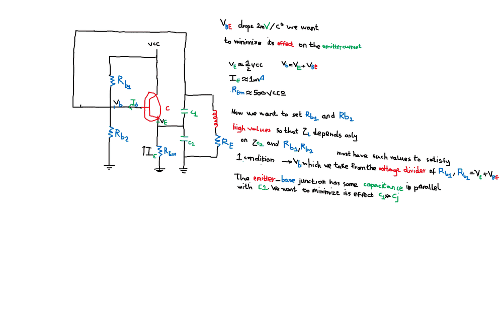
When we design a Colpitts oscillator we must set the value of C1 to be bigger than the parasitic capacitance of the emitter base junction. However in a Hartley oscillator we have an inductive voltage divider and I was wondering if we should put a big inductor (0.1H) in parallel with L1 because Lj = 0 -> L1||Lj = 0;
 
Engineering news on Phys.org
  • #2
Adding an inductor in parallel with L1 would change the frequency of the tank circuit. Not to sure about adding an inductor in series with RE. Seems like you add extra impedance to ground which would make the oscillator noisy.
 
  • #3
We still need as much capacitance as possible across E-B to swamp out the parasitic capacitance. If it is too high, oscillation will stop due to low gain. If it is too low, the frequency stability will be poor.
 
  • #4
tech99 said:
We still need as much capacitance as possible across E-B to swamp out the parasitic capacitance. If it is too high, oscillation will stop due to low gain. If it is too low, the frequency stability will be poor.
tech99 capacitances in parallel are added , while inductances in series are the same with the resistances so adding a capacitor to the LC oscillator will just make it more capacitive and less inductive
 
  • #5
We adjust the product of L and C to obtain the required frequency. When we increase C to improve stability, we must reduce L to bring the frequency correct.
 
  • #6
It's been decades since I looked at colpitts/hartley oscillators with BJTs, since it is ancient technology; you won't see it in the real world. But... you absolutely will see the concepts of tanks and phase-shifted feedback, so it is good to study. Anyway, take my comments with a grain of salt, so to speak.

BJTs have junction capacitance, all of them, it is intrinsic to the device, what with depletion regions and such. But they are small things, so parasitic inductance in the actual semiconductor can nearly always be ignored. We do worry about the inductance of the leads going into the device at high frequencies, but that is best thought of as "wiring" like the trace in your schematic between components. OTOH, in high frequency designs, everything is like a transmission line with inductance and capacitance everywhere that can't be ignored.

In you're schematic C1 is in parallel with the Cbe device capacitance. So I think they want it to be big to overcome any junction capacitance variations (part to part, temperature, or as the junction capacitance changes with charge distribution). Stable oscillators need stable tank components.

BTW, that isn't what I think of as a Colpitts oscillator, since there's no real voltage feedback from the collector, I guess they are using current gain from the emitter? But that doesn't mean it isn't, I haven't really analyzed it.

I thought these were some good descriptions:
https://www.electronics-tutorials.ws/oscillator/hartley.html
https://www.electronics-tutorials.ws/oscillator/colpitts.html
 
  • #7
DaveE said:
It's been decades since I looked at colpitts/hartley oscillators with BJTs, since it is ancient technology; you won't see it in the real world. But... you absolutely will see the concepts of tanks and phase-shifted feedback, so it is good to study. Anyway, take my comments with a grain of salt, so to speak.

BJTs have junction capacitance, all of them, it is intrinsic to the device, what with depletion regions and such. But they are small things, so parasitic inductance in the actual semiconductor can nearly always be ignored. We do worry about the inductance of the leads going into the device at high frequencies, but that is best thought of as "wiring" like the trace in your schematic between components. OTOH, in high frequency designs, everything is like a transmission line with inductance and capacitance everywhere that can't be ignored.

In you're schematic C1 is in parallel with the Cbe device capacitance. So I think they want it to be big to overcome any junction capacitance variations (part to part, temperature, or as the junction capacitance changes with charge distribution). Stable oscillators need stable tank components.

BTW, that isn't what I think of as a Colpitts oscillator, since there's no real voltage feedback from the collector, I guess they are using current gain from the emitter? But that doesn't mean it isn't, I haven't really analyzed it.

I thought these were some good descriptions:
https://www.electronics-tutorials.ws/oscillator/hartley.html
https://www.electronics-tutorials.ws/oscillator/colpitts.html
I am not asking about this schematic just imagine if you replace C1 and C2 with L1 and L2 and L1 with C1 why don't we add an inductor in series with the Rem
 
  • #8


It says when he is talking about the parasitic capacitance of the BE junction that we choose C1 to have such a value that any changes in Cj won't affect the circuit. If we have a Hartley oscillator why don't we put a fairly big inductor in series with L1 (in place of C1) because the total inductance of between base-emitter will be 0 if we don't to make it roughly equal to L1?
 
  • #9
I like your understanding of the duality of these two oscillators.

The key point in both is using a highly resonant LC tank to provide phase shifted feedback to an amplifier. One gets that phase shift by tapping the tank between two capacitors, the other between two inductors.

Other stipulations, like the large C1 comment, are not fundamental to the topology. Those are implementation details more associated with the amplifier than the oscillator tank. You won't see that particular limitation with other amplifier configurations. That is why in the real world, that transistor amplifier will be an IC, like an op-amp, which is easier to use and has better performance than a single BJT. If I was teaching feedback oscillators, I wouldn't combine it with single BJT amplifiers because of this added complexity.

I guess the more general point is that for a tank feedback oscillator to work well, the tank reactance needs to be stable, and the tank needs to not be excessively loaded by the stuff connected to it to damp the resonance. You can think of this as input and output impedance requirements on the amplifier. The duality you have identified in the two tank configurations isn't matched with duality of the amplifier stage, so the interface between the tank and the amp isn't necessarily the same (or dual).
 
  • #10
DaveE said:
I like your understanding of the duality of these two oscillators.

The key point in both is using a highly resonant LC tank to provide phase shifted feedback to an amplifier. One gets that phase shift by tapping the tank between two capacitors, the other between two inductors.

Other stipulations, like the large C1 comment, are not fundamental to the topology. Those are implementation details more associated with the amplifier than the oscillator tank. You won't see that particular limitation with other amplifier configurations. That is why in the real world, that transistor amplifier will be an IC, like an op-amp, which is easier to use and has better performance than a single BJT. If I was teaching feedback oscillators, I wouldn't combine it with single BJT amplifiers because of this added complexity.

I guess the more general point is that for a tank feedback oscillator to work well, the tank reactance needs to be stable, and the tank needs to not be excessively loaded by the stuff connected to it to damp the resonance. You can think of this as input and output impedance requirements on the amplifier. The duality you have identified in the two tank configurations isn't matched with duality of the amplifier stage, so the interface between the tank and the amp isn't necessarily the same (or dual).
Ah ok so we don't need to put any inductor. Thanks Dave for the comments!
 
  • #11
In the OP schematic, L and RE short the base bias to ground.
There seems to be an isolation capacitor missing from the C2 to ground connection, or from the base bias circuit.
 
  • #12
Baluncore said:
In the OP schematic, L and RE short the base bias to ground.
There seems to be an isolation capacitor missing from the C2 to ground connection, or from the base bias circuit.
Yes, it's not right. I think they meant this configuration:
https://www.electrical4u.com/images/march16/1469259519.PNG
 
  • #13
DaveE said:
It's been decades since I looked at colpitts/hartley oscillators with BJTs, since it is ancient technology; you won't see it in the real world.
During the 1980's and into the 1990's Colpitts osc's were in every transmitter line up and receiver LO in
commercial transceivers I worked on during that time. In the early-mid 1990's the PLL VCO's became the way to go
 
  • #14
Picture of stable Hartley oscillator using vacuum tube which I recently made.
 

Attachments

  • vfo 002.JPG
    vfo 002.JPG
    107.4 KB · Views: 162
  • vfo 001.JPG
    vfo 001.JPG
    75.3 KB · Views: 129
  • #15
Baluncore said:
In the OP schematic, L and RE short the base bias to ground.
There seems to be an isolation capacitor missing from the C2 to ground connection, or from the base bias circuit.

In the video the guy tests it with a multimeter and it shows stable oscillations -> it must be correct.
 
  • #16
Baluncore said:
In the OP schematic, L and RE short the base bias to ground.
There seems to be an isolation capacitor missing from the C2 to ground connection, or from the base bias circuit.
DaveE said:
Yes, it's not right. I think they meant this configuration:
https://www.electrical4u.com/images/march16/1469259519.PNG
C3 is just a bypass capacitor for AC signals.
 
  • #17
Helena Wells said:
In the video the guy tests it with a multimeter and it shows stable oscillations -> it must be correct.
I don't know which circuit diagram, or which component is being discussed, so I really can't comment until I see a diagram with real component identifiers and values.
 
  • #18
Baluncore said:
I don't know which circuit diagram, or which component is being discussed, so I really can't comment until I see a diagram with real component identifiers and values.
Rb1 and Rb2 is 82k and 100kOhms and Rem = 4.7KOhm with a VCC of 9V
 
  • #19
Helena Wells said:
Rb1 and Rb2 is 82k and 100kOhms and Rem = 4.7KOhm with a VCC of 9V
I assume you are referring to the schematic in post #1.
What is the value of RE ?
Helena Wells said:
C3 is just a bypass capacitor for AC signals.
You do not show a C3 on the schematic in post #1.
 
  • #20
Re is the parasitic resistance of the inductor , it is small put it 10 Ohms. And we don't necessarily need a bypass capacitor
 
  • #21
Helena Wells said:
Re is the parasitic resistance of the inductor , it is small put it 10 Ohms.
10 ohms is a huge of series resistance. I would expect about one ohm.
What you are saying is that the base of the transistor is connected through an inductor with little series resistance to ground. Follow the feedback wire and you will see that the base bias is not being set by Rb1 and Rb2. Go back and check the original source.
 
  • #22
Yes I see it too now.We have a very small resistance in parallel with a huge resistance so the small resistance will short the circuit.But in the video he uploads that schematic and using the multimeter it seems to work.
 
  • #23
Helena Wells said:
But in the video he uploads that schematic and using the multimeter it seems to work.
But we know it cannot work because the transistor is biassed off.
 
  • #24
Baluncore said:
But we know it cannot work because the transistor is biassed off.
Ya that's very odd.
 
  • #25
When you add C3, the bias works OK and it oscillates as expected.

schematic+C.png


Plot.png
 
  • Like
Likes DaveE and jim mcnamara
  • #26
How it isn't an underdamped oscillation since you set the feedback fraction equal to 1??
 
  • #27
Helena Wells said:
How it isn't an underdamped oscillation since you set the feedback fraction equal to 1??
C1 and C2 make a potential divider. With L, that makes a centre tapped resonant circuit. Relative to ground, the voltage at the top of C1 is twice the voltage at the bottom of C1, so the feedback gain is closer to two. It actually has too much gain and needs C3 to be reduced to 10 pF, and Rem increased to 15k. That both reduces distortion, plus oscillation starts and stabilises faster.

LTspice is a free simulator from Analog Devices Inc. If you get a copy I will post the simulation file for the Colpitts oscillator so you can test your ideas directly.
https://www.analog.com/en/design-center/design-tools-and-calculators/ltspice-simulator.html
https://en.wikipedia.org/wiki/LTspice
 
  • #28
Baluncore said:
C1 and C2 make a potential divider. With L, that makes a centre tapped resonant circuit. Relative to ground, the voltage at the top of C1 is twice the voltage at the bottom of C1, so the feedback gain is closer to two. It actually has too much gain and needs C3 to be reduced to 10 pF, and Rem increased to 15k. That both reduces distortion, plus oscillation starts and stabilises faster.

LTspice is a free simulator from Analog Devices Inc. If you get a copy I will post the simulation file for the Colpitts oscillator so you can test your ideas directly.
https://www.analog.com/en/design-center/design-tools-and-calculators/ltspice-simulator.html
https://en.wikipedia.org/wiki/LTspice
Isn't the feedback fraction C1/C2? If C1 = C2 then the feedback fraction must be equal to 1.
 
  • #29
Baluncore said:
C1 and C2 make a potential divider. With L, that makes a centre tapped resonant circuit. Relative to ground, the voltage at the top of C1 is twice the voltage at the bottom of C1, so the feedback gain is closer to two. It actually has too much gain and needs C3 to be reduced to 10 pF, and Rem increased to 15k. That both reduces distortion, plus oscillation starts and stabilises faster.

LTspice is a free simulator from Analog Devices Inc. If you get a copy I will post the simulation file for the Colpitts oscillator so you can test your ideas directly.
https://www.analog.com/en/design-center/design-tools-and-calculators/ltspice-simulator.html
https://en.wikipedia.org/wiki/LTspice
And C1 with C2 don't make a voltage divider. You forgot about L1.And C1 is in series with C2 so the total capacitance is C1*C2/C1+C2
 
  • #30
Baluncore said:
C1 and C2 make a potential divider. With L, that makes a centre tapped resonant circuit. Relative to ground, the voltage at the top of C1 is twice the voltage at the bottom of C1, so the feedback gain is closer to two. It actually has too much gain and needs C3 to be reduced to 10 pF, and Rem increased to 15k. That both reduces distortion, plus oscillation starts and stabilises faster.

LTspice is a free simulator from Analog Devices Inc. If you get a copy I will post the simulation file for the Colpitts oscillator so you can test your ideas directly.
https://www.analog.com/en/design-center/design-tools-and-calculators/ltspice-simulator.html
https://en.wikipedia.org/wiki/LTspice
I have downloaded LTSpice and I am using it .Please post the LTSpice file please.
 
  • #31
Helena Wells said:
Isn't the feedback fraction C1/C2? If C1 = C2 then the feedback fraction must be equal to 1.
And yet it oscillates. There are many configurations. The feedback gain will depend on how the resonant circuit is grounded.

Helena Wells said:
You forgot about L1
No I didn't. The resonant circuit or "tank" is L in parallel with C1 and C2 in series. One side of L is grounded. The top of L is connected to the base. Half the AC appears across each capacitor, so it acts like a centre tapped "transformer". The emitter drive to the centre tap is effectively doubled to the base.

Spice files attached. To run the .asc file with LTspice, remove the .txt extension that allows me to attach the ascii file to a post. Do the same with the .plt file to get the same traces and colours I get.
 

Attachments

  • Colpitts_V_2.asc.txt
    1.7 KB · Views: 127
  • Colpitts_V_2.plt.txt
    349 bytes · Views: 148
  • #32
Helena Wells said:
Isn't the feedback fraction C1/C2? If C1 = C2 then the feedback fraction must be equal to 1.
You must consider all of the components in the feedback network, theoretically that's every passive component for this configuration*. However, the resistor values are really big and can be ignored, they will have a negligible effect.

One shortcut you can use for a circuit that you know is supposed to work at a particular frequency (in this case you can guess that it will be the LC tank resonant frequency) is to quickly determine the magnitude of the impedances of the parts and compare them. You don't have to be too accurate, you're just looking for really big differences that may allow you to eliminate some from your thinking about what matters. Similar to the way you may separate DC bias calculations from AC dynamic calculations.

Also, for circuits that operate at resonance, you know that the inductive impedance magnitude(s) are the same as the capacitive impedance magnitudes (that's always the situation at resonance). So, for a circuit like this one, you can very quickly identify that Zo=√(L/C), the characteristic impedance of the tank (which is the magnitude of the L or C impedance at resonance), is the significant impedance for the whole dynamic circuit.

You will save yourself a lot of effort in the future if you just memorize the resonant frequency and characteristic impedance of LC tanks:

ωo=1/√(LC) and Zo=√(L/C), also Q=Zo/R (series LCR) or Q=R/Zo (parallel LCR) for lossy circuits (which isn't really applicable, in this case).

*post #25, @Baluncore simulation.
 
Last edited:
  • #33
Helena Wells said:
Ya that's very odd.
The transistor has no bias applied, so it is cut-off and in Class C. No collector current will flow until oscillation starts, then current will flow on positive half cycles. Such oscillators will not start without an intial kick, which might occur due to the switch-on impulse or due to someone touching the circuit.
 
  • #34
tech99 said:
Such oscillators will not start without an intial kick, which might occur due to the switch-on impulse or due to someone touching the circuit.
You are correct. Without C3 to float the base voltage the circuit can still maintain oscillation, but it will not start without an initial current pulse in L, or a high voltage applied to the shorted base, neither of which is going to happen in a real implementation of the circuit.

If it could start without C3, the base-emitter junction would then regulate amplitude by entering reverse breakdown at about -5V on each cycle, which is not good for transistor health.
 
  • Like
Likes DaveE
  • #35
Baluncore said:
You are correct. Without C3 to float the base voltage the circuit can still maintain oscillation, but it will not start without an initial current pulse in L, or a high voltage applied to the shorted base, neither of which is going to happen in a real implementation of the circuit.

If it could start without C3, the base-emitter junction would then regulate amplitude by entering reverse breakdown at about -5V on each cycle, which is not good for transistor health.
I tend to think that even with corect bias, the device will tend to
Baluncore said:
When you add C3, the bias works OK and it oscillates as expected.

View attachment 277128

View attachment 277130
How can 35mA flow through he 4.7k emitter resistor with a supply of 9 volts?
 

Similar threads

Replies
4
Views
4K
Replies
11
Views
14K
  • Electrical Engineering
Replies
14
Views
4K
  • Electrical Engineering
Replies
4
Views
6K
  • Electrical Engineering
Replies
1
Views
3K
  • Electrical Engineering
Replies
3
Views
3K
  • Introductory Physics Homework Help
Replies
10
Views
2K
  • Introductory Physics Homework Help
Replies
8
Views
8K
  • Electrical Engineering
Replies
1
Views
5K
  • Electrical Engineering
Replies
18
Views
6K
Back
Top