How does electric current distribute through a conductor?

5 replies · 2K views · last reply
Another
Messages
104
Reaction score
5
TL;DR
What happens when electric current is distributed in the material(Non-metal)?
When supplying electricity to the material. the shape of the material may or may not be square.
This material may be

This material may be moisture materials or solid materials that may conduct electricity.
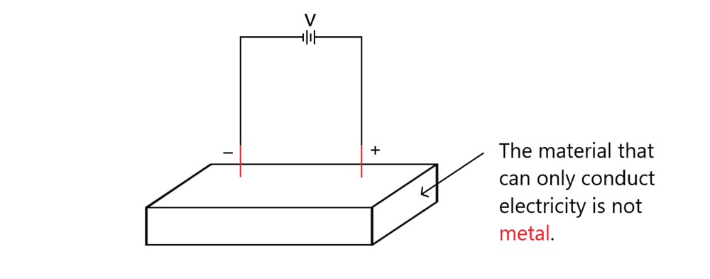
Diagram of a rectangular slab of material with two red electrode contacts on its top face, marked minus and plus, connected by wires to a battery labelled V; a note says the material that can only conduct electricity is not metal.

I would like to know the travel characteristics of electric currents and the potential difference in each position of the material.
How will be distributed?
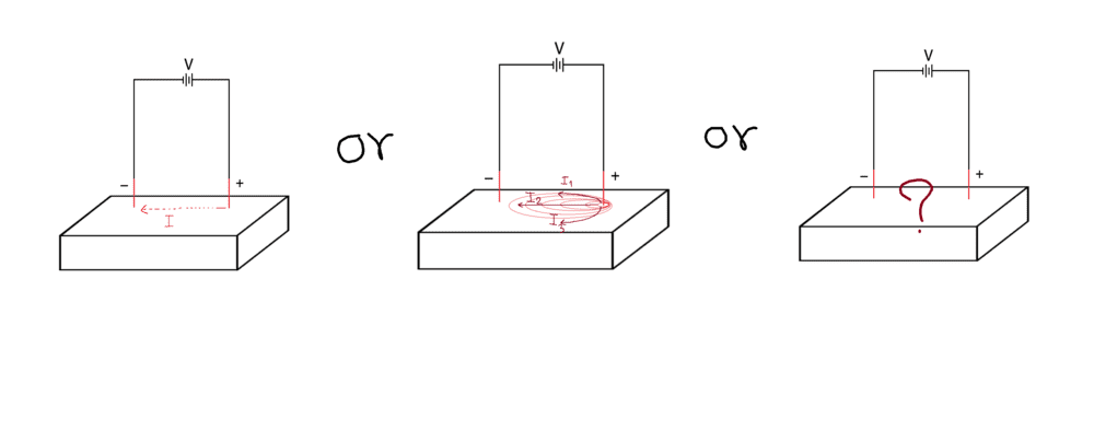
Three sketches of a rectangular block with a battery across two electrodes on its top face: left, a single straight red dashed current arrow between electrodes; middle, curved red current loops with labels I1 and I2; right, a question mark between the electrodes.


Is there a topic or theory that explains this behavior? Please advise me to study.
 
I believe that the vector form of Ohm's law in combined with Ampere's circuital law can be applied.

J = σ E

where J is the current density at a given location in a resistive material, E is the electric field at that location, and σ (sigma) is a material-dependent parameter called the conductivity
 
Last edited:
  • Like
Likes   Reactions: Another
Another said:
Summary:: What happens when electric current is distributed in the material(Non-metal)?

I would like to know the travel characteristics of electric currents and the potential difference in each position of the material.
How will be distributed?
Well, that depends on the state of the material and the environment. A research institute I worked for 40 years ago used this principle for detecting internal cracks in oil pipes. You run a high current through the material and measure the magnetic field between the poles (the current and the field will "wrap around" any cracks).
 
  • Like
Likes   Reactions: sysprog
Another said:
Summary:: What happens when electric current is distributed in the material(Non-metal)?

I would like to know the travel characteristics of electric currents and the potential difference in each position of the material.
How will be distributed?
That's not a simple question. By the way, you have a 3D object, not 2D.

Semiconductor device designers consider exactly that question. For example:

Cross-section simulation of a MOS transistor showing colour-mapped current flow lines from 0 to 0.937, with Gate, Source and Drain labelled, SiO2, silicon, polysilicon and aluminium regions, and axes in micrometres.


There are also analytic methods as in
https://www.google.com/url?sa=i&sou...aw19xF9WbQbgd0CFFKQrv87b&ust=1576769471286070
Two diagrams of field lines around a cross-shaped conductor: (a) horizontal lines bending around a cross-shaped conductor; (b) vertical curved lines around a gap between two conductors, labelled (a) and (b).

https://www.google.com/url?sa=i&sou...aw19xF9WbQbgd0CFFKQrv87b&ust=1576769471286070

If the external voltage is not constant in time, there are also eddy currents, surface currents, and transient solutions to consider. This is no simple answer to your question. I expect that many PhD theses have been written on that question.
 
  • Like
Likes   Reactions: Lord Jestocost and sysprog
Another said:
I would like to know the travel characteristics of electric currents and the potential difference in each position of the material.

One way to approximately get such data is an equivalent circuit simulation by modelling the material as a 3D resistor network.
 
  • Like
Likes   Reactions: anorlunda
A point has no area so the resistance of a point contact is infinite. The current density at a point contact is also infinite. While voltage measurements can be made at points, the current density pattern in a resistive material must be specified between defined contact areas, not between point contacts.

Analytic solutions require restriction of the contact areas and boundary conditions to idealised geometry.

Electric field patterns and current flow in real-world bounded-solids are often solved using finite element numerical relaxation techniques.