How Transistor works - verifying

  • Thread starter Thread starter Nikarus
  • Start date Start date
  • Tags Tags
    Transistor Works
Click For Summary
SUMMARY

This discussion centers on the operation of NPN transistors, specifically the interaction between the emitter, base, and collector regions under varying voltage conditions. Key points include the formation of depletion layers without voltage, the role of controlling voltage at the base to allow current flow from emitter to collector, and the importance of a thin base for effective current amplification. Participants emphasize the significance of understanding the injection and transport components of base current, as well as the impact of frequency on current gain.

PREREQUISITES
  • Understanding of semiconductor physics, particularly the behavior of NPN transistors.
  • Familiarity with terms such as depletion layers, majority and minority carriers, and current amplification.
  • Knowledge of voltage biasing in transistor operation, including forward and reverse biasing.
  • Basic comprehension of current gain metrics, including hFE and beta values.
NEXT STEPS
  • Study the principles of BJT operation, focusing on the role of the base-emitter and base-collector junctions.
  • Learn about the impact of frequency on transistor performance and current gain.
  • Explore peer-reviewed literature on semiconductor devices to gain a deeper understanding of current amplification mechanisms.
  • Investigate the differences between BJTs and FETs, particularly in terms of current control and operational characteristics.
USEFUL FOR

Electronics students, engineers, and hobbyists seeking to deepen their understanding of transistor operation and current amplification mechanisms.

Nikarus
Messages
10
Reaction score
0
Hi All,
I'm trying to understand how transistor works. I have drew some pictures for NPN transistor to show my current understanding. Can you please verify this for me.
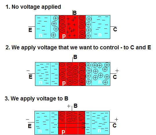
npn.PNG


On the picture:
"-" and "+" are movable charges;
circled "-" and circled "+" are immovable ions.

1. No voltage applied. Two depletion layers are formed.

2. We apply voltage that we want to control - "-" to Emitter and "+" to Collector. Electrons from Emitter fill the Base forming negative ions. Electrons from Collector are gone; positive ions are formed in there. Because Base is filled with negative ions, electrons from Emitter can't go through - channel jammed.
Here I'm not sure about Base-Emitter depletion layer - will there be any interaction between Base and Collector..?

3. We apply controlling voltage to Base. If we have BJT than we will have current between Base and Emitter, if we have FET, electrons inside of Base will be just pulled up, leaving positive charges behind. Electrons from Emitter will flow thought Base to Collector and will not be jammed again because Base is very thin.

So, is my understanding correct? Do I do any mistakes..?
Thank you!
 
Last edited:
Engineering news on Phys.org
Guys please, I spent a lot of time drawing this picture!
 
you can look at transistor as two diodes facing each other

--l>l-*-l<l---


this also forms NPN junction and will let thru if voltage is applied to the between.

Your assumption is basically correct ~ Applying + to emmiter will draw free electrons from there leaving + ions, applying - to collector will result in moving electrons to base and neutralizing some free 'holes'.
And when applying + to base most of electrons will go from collector to emmiter, but some will go to + in base and coming back to collector, so the smaller is base the better.
In ideal transistor Electron flow input in collector should = electron output in emmiter.
 
Tryp said:
you can look at transistor as two diodes facing each other

--l>l-*-l<l---

that's hardly the case. it doesn't account at all for the mechanism of current amplification due to the thin base.

indeed...

And when applying + to base most of electrons will go from collector to emmiter, but some will go to + in base and coming back to collector, so the smaller is base the better.

you won't get a thin base layer by soldering two diodes facing each other.
 
rbj said:
that's hardly the case. it doesn't account at all for the mechanism of current amplification due to the thin base.

it will work out transistor mechanism just fine.

rbj said:
you won't get a thin base layer by soldering two diodes facing each other.
never said so.
 
It's difficult to find a good explanation about transistors, but here a link

<< link deleted by berkeman >>

It's a big article, but it leaves most questions behind once you read it.
 
Last edited by a moderator:
I've posted this here several times. I hope it might help your understanding.

tran10.gif


http://hyperphysics.phy-astr.gsu.edu/hbase/solids/trans2.html"
 
Last edited by a moderator:
valeriy2222 said:
It's difficult to find a good explanation about transistors, but here a link

<< link deleted by berkeman >>

It's a big article, but it leaves most questions behind once you read it.

This article is heresy. Peer-reviewed texts have the best info. I've covered this issue many times as well as others. A search for my post history will show these threads. Then I can address any questions. Stay away from the above web site. It contains just enough truth to look credible, but makes assumptions contrary to known science.

Claude
 
Last edited by a moderator:
Hi All,
Sorry for the delay - I had a lot of thing to do these days. But I'm still full of enthusiasm :)
I tried to read this explanation before (<< link deleted by berkeman >>) And I agree with author that a lot of other authors does not really explain how transistors work. But since cabraham says that this is heresy, I stopped reading it :)

Actually I already read a lot of explanations about how transistor works, and I have my understanding. And I want to make sure of it. So this is why I posted this thread.

Guys, please, can you not just give me another explanations, but read my own and tell me what is wrong there on my picture. So I could use my own understanding as a reference point to move from.
 
Last edited by a moderator:
  • #10
cabraham said:
This article is heresy. Peer-reviewed texts have the best info. I've covered this issue many times as well as others. A search for my post history will show these threads. Then I can address any questions. Stay away from the above web site. It contains just enough truth to look credible, but makes assumptions contrary to known science.

Claude

Among other explanations this one gives you an understanding of principle of work. Having read this, you can correct mistakes made in the article by reading other more scientific articles and thus come up with the whole and right picture.
 
  • #12
valeriy2222 said:
Among other explanations this one gives you an understanding of principle of work. Having read this, you can correct mistakes made in the article by reading other more scientific articles and thus come up with the whole and right picture.

Sure, but why not just read more scientific articles in the 1st place that don't have mistakes. Then there is no need to correct them. Peer-reviewed books from semiconductor producers & universities are the best source of info. These contrarian web sites just confuse the issue to the point where one does not know who to believe.

Claude
 
  • #13
Nikarus said:
Hi All,
Sorry for the delay - I had a lot of thing to do these days. But I'm still full of enthusiasm :)
I tried to read this explanation before (<< link deleted by berkeman >> ). And I agree with author that a lot of other authors does not really explain how transistors work. But since cabraham says that this is heresy, I stopped reading it :)

Actually I already read a lot of explanations about how transistor works, and I have my understanding. And I want to make sure of it. So this is why I posted this thread.

Guys, please, can you not just give me another explanations, but read my own and tell me what is wrong there on my picture. So I could use my own understanding as a reference point to move from.

In your pic, 3rd view at bottom, the base region is shown w/ an excess of electrons, herein called "e-", & an absence of holes herein "h+". Also, the collector has many e-, but few h+.

For the 3rd pic, where Vce > 0, & Vbe > 0, the device is in its active region. We will not cover the saturated region yet. In the collector, there are a small number of mobile h+, as they are minority carriers, & e- are majority carriers w/ high mobility. W/o Vbe biased > 0, the e- are crowded near the collector lead, & the h+ are near the base-collector boundary. The c-b jcn is rev biased & little current exists from base to collector.

But the b-e jcn is now fwd biased from an external source, & Ib/Ie > 0, & Vbe > 0. The emitter emits many e- toward the base, & the base emits not as many h+ towards the emitter. The h+ from the base enter the emitter & recombine w/ e- near the e-b boundary. The e- from the emitter transit into the base region. Some recombine w/ a h+ in the base, some transit through the base region out the base lead, & nearly all transit through the base into the collector region, where they again are majority carriers.

The number of e- which do not reach the collector are around 1 in 2000 to 1 in 5000. The number of h+ emitted from the base are about 100 to 200 times less than the number of e- emitted from the emitter. Thus the base current consists chiefly of holes emitted from base to emitter. This is the injection component of base current. The e- emitted from the emitter which recombine in base or exit base lead constitute a very small fraction of the base current & is called the transport component.

Another component of base current is the charging or displacement component. As frequency increases more h+ & e- get displaced but do not contribute to collector current. So the current gain decreases as freq increases. Eventually there is a frequency where the beta value equals one. This is the transition frequency of the bjt, called "ft" on data sheets.

The injection & transport components of base current determine the dc & low freq current gain, "hFE" on spec sheets. Adding the displacement component of base current decreases the current gain (beta value) at high freq. The ac & high freq current gain is called "hfe" on spec sheets.

It's all about the c-b jcn being reverse biased so that very little collector current exists. By forward biasing the b-e jcn, many e- flow from emitter to base. Nearly all are yanked into the collector by the electric field in the b-c boundary region. The base is made thin so as to minimize the number of e- recombining in base region. The base is doped lightly & the emitter heavy so as to minimize the injection component of base current.

The current gain, bets, is determined by Ic/Ib, where Ib consists of the 3 parts, injection, transport, & displacement.

Regarding heresy, I've addressed Mr. Beaty on another forum. We had a debate. I'll provide a link if you wish to see the points he & I presented.

Best regards.

Claude
 
Last edited by a moderator:
  • #14
Hi Claude,

I'm very interested in the debate you had with Mr. Beaty. Can you post the link? :)
 
  • #16
Man, I can't believe you guys had the patience to duke it out like that! And it ended with some level of agreement? Truly epic.

I actually enjoyed reading Mr. Beaty's site, but there should be a rebuttal to it, or a summary of the epic thread published on the web. I think a lot of confused people would appreciate it. Thanks for sharing.
 
  • #17
niwin said:
Man, I can't believe you guys had the patience to duke it out like that! And it ended with some level of agreement? Truly epic.

I actually enjoyed reading Mr. Beaty's site, but there should be a rebuttal to it, or a summary of the epic thread published on the web. I think a lot of confused people would appreciate it. Thanks for sharing.

One of these days I should copy & paste the whole thread into a text document. Then I can post the text. It gives all the different viewpoints from many different parties. That way, nobody is quoted out of context. I'll do that soon.

Claude
 
  • #18
niwin said:
Hi Claude,

I'm very interested in the debate you had with Mr. Beaty. Can you post the link? :)

I'm interested too, since I've never had any such debate.
 
  • #19
wbeaty said:
I'm interested too, since I've never had any such debate.

Refer to the link I gave a few posts back. The poster called himself Bill Beaty. Once again, here it is:

http://www.electro-tech-online.com/g...voltage-4.html

If that isn't you, then someone used your name. Maybe the moderators on that forum can help you. Best regards.

Claude
 
Last edited by a moderator:
  • #20
Last edited by a moderator:
  • #21
There have been other web debates about Beaty's site.

In general you cannot divorce voltage and current. So to claim that a transistor is wholely current controlled or wholely voltage controlled is pointless to say the least.

In this thread I pointed out that there are other ways to affect (control) the collector current than either changing the voltage or injecting base current.

One way is by injecting photons which increase the base current without increasing the base voltage and thereby increase the collector current.

http://forum.allaboutcircuits.com/showthread.php?t=12378&highlight=transistor+action&page=13
 
  • #22
Since you gave this link Studiot, I checked it out and one thing caught my eye. Discussion between Ebers-Moll and Gummel-Poon. I learned Gummel-Poon model of bipolar transistor at my college, and I know how to derive them from scratch. I see something about frequencies being mentioned.

Is this only limitation of this GP model? And which model generally is more accurate?
 
  • #23
wbeaty said:
I did.


Where? No "beaty" at all on that page linked above, or on that thread as far as I've searched. On that site I see you debating with a "Ratchit"

Sorry, I gave the wrong link. Here is the discussion you & I had, along w/ others, back in 2010:

https://www.physicsforums.com/showthread.php?t=390291&highlight=wbeaty

Again, my apologies. Best regards.

Claude
 
  • #24
Studiot said:
In this thread I pointed out that there are other ways to affect (control) the collector current than either changing the voltage or injecting base current.

One way is by injecting photons which increase the base current without increasing the base voltage and thereby increase the collector current.
Wow, interesting! Have some evidence that it happens as you say? Opto engineering refs about this issue?

Or forget talking, "Let the experiment be made." Instead just take a phototransistor and go see what actually happens. Try using a variable DC supply to hold the Vbe constant while flashing a light source and measuring Ie or Ic pulse. Then do it again with a floating Base lead. The usual BJT models predict that any expected large gain in current during the light pulse cannot occur if the height of the potential barrier at the BE junction isn't allowed to change. The Emitter won't be commanded to emit. Obviously you'll still get a photocurrent. But if the BE junction barrier is fixed, there shouldn't be any transistor action or any large emitter current.

Full disclosure: I spent some years as an EE at Eaton/Cutler-Hammer photosensors division. But PTs don't have well controlled characteristics, so all our products employed Photodiodes (PDs,) so I wouldn't have encountered this weird "no Vbe change" phototransistor phenomenon.
Studiot said:
http://forum.allaboutcircuits.com/showthread.php?t=12378&highlight=transistor+action&page=13

Nothing about phototransistors that I find. Page 13 wrong?
 
Last edited:
  • #25
@wbeaty

Posts 55/66/80/84 in the link contain the information you asked for. You can get a photon induced variation to collector current without the base even being connected, let alone arguing whether it is current or voltage controlled.
I do not recommend this but there used to be a demonstration involving sawing the top off a 2N3055 and shining a light on it. Scratching an old glass-cased germanium transistor is a safer bet.

@bassalisk

Gemmel- Poon is some way beyond Ebbers Moll and is a good model over a wider current range and frequency range and certainly well beyond anything you have discussed here at PF before.
Both are circuit theory models, not models of the physics of transistors. You should always distinguish which you are needing or considering.
 
  • #26
Studiot said:
@wbeaty
Posts 55/66/80/84 in the link contain the information you asked for.

Thanks, I'll check it out

Studiot said:
You can get a photon induced variation to collector current without the base even being connected

Certainly, that's how 2-lead phototransistors are supposed to work. The base must remain disconnected in order to let Vbe vary freely. On a 3-lead PT you can use a voltmeter to watch the changes. But if we use a power supply to hold Vbe constant, will the large transistor-effect current vanish?


Studiot said:
demonstration involving sawing the top off a 2N3055

Nah, the ambitious or curious could just buy reliable devices designed for the task:

http://search.digikey.com/scripts/DkSearch/dksus.dll?vendor=0&keywords=phototransistors+ssg+through+hole&stock=1"J

http://www.mouser.com/Optoelectronics/Optical-Detectors-and-Sensors/Photodetector-Transistors/_/N-6jjuf?Keyword=osram&FS=True"
 
Last edited by a moderator:
  • #27
wbeaty said:
Wow, interesting! Have some evidence that it happens as you say? Opto engineering refs about this issue?

Or forget talking, "Let the experiment be made." Instead just take a phototransistor and go see what actually happens. Try using a variable DC supply to hold the Vbe constant while flashing a light source and measuring Ie or Ic pulse. Then do it again with a floating Base lead. The usual BJT models predict that any expected large gain in current during the light pulse cannot occur if the height of the potential barrier at the BE junction isn't allowed to change. The Emitter won't be commanded to emit. Obviously you'll still get a photocurrent. But if the BE junction barrier is fixed, there shouldn't be any transistor action or any large emitter current.

Full disclosure: I spent some years as an EE at Eaton/Cutler-Hammer photosensors division. But PTs don't have well controlled characteristics, so all our products employed Photodiodes (PDs,) so I wouldn't have encountered this weird "no Vbe change" phototransistor phenomenon.

But we DO NOT ever hold Vbe constant. That is the point of controlling current, not voltage. When a bjt is *current driven*, the source providing the current also provides the voltage. In the case of current controlling a b-e jcn of a bjt, it is understood, no need to explicitly state, that a change in Ib/Ie inevitably produces a change in Vbe as well.

Nothing about phototransistors that I find. Page 13 wrong?

I'm not sure what you're trying to prove by holding Vbe steady with a dc lab constant voltage supply clamped right acrss the b-e jcn. That is not how to drive it. I believe that what you are demonstrating is that when photons are incident upon the jcn, & current is set up in response to the photon stimulus, that there will inevitably be a change in Vbe. Is that your point?

But I would have told you the same, as would many others here skilled in semicon physics. Once carriers are emitted from the emitter & base regions, they cross the barrier & recombination/ionization takes place. There is a change in the local E field due to this increased density of carriers. Since Vbe is just the line integral of the E field along the b-e path, a change in Ib/Ie results in a change in the net E field in the depletion zone, which results in a change in Vbe.

Whenever bjt action takes place, all quantities participate, namely Ib, Vbe, Ie, & Vbc. "Transistor action" requires all of them. The "current control" description we use, refers to the quantity that is directly controlled, & it is understood that the others are incidental, but still participate. We control Ie, or in limited applications we control Ib. But Vbe is indirect & consequential, although it is still an important parameter.

If we wish to use a bjt to run a motor requiring 1.0 amp, with a beta of 100, Si bjt material, then we need 10 mA & 0.65 volts to operate the bjt. Again, we DO NOT apply a 0.65V voltage source to the jcn, but rather we apply 10 mA to the jcn, & let Vbe fall where it may. At different temperatures Vbe will vary. But Vbe is important, very much so. If the source providing the 10 mA of base drive, has a maximum voltage compliance of just 0.40 volt, then we are out of luck. Ib & Vbe are both needed, but only 1 can be the directly controlled quantity.

Have I explained myself well? Further questions/comments are welcome.

Claude
 
  • #28
cabraham said:
Once carriers are emitted from the emitter & base regions, they cross the barrier & recombination/ionization takes place. There is a change in the local E field due to this increased density of carriers. Since Vbe is just the line integral of the E field along the b-e path, a change in Ib/Ie results in a change in the net E field in the depletion zone, which results in a change in Vbe.

Will Studiot agree? I was responding to his earlier message asserting that, when illumination is applied to a phototransistor, Vbe doesn't change.

BTW, my training background is BSEE, the usual 4-year degree. What's yours? (If you're remaining anonymous, no need to give personal info.)
 
Last edited:
  • #29
wbeaty said:
Will Studiot agree? I was responding to his earlier message asserting that, when illumination is applied to a phototransistor, Vbe doesn't change.

BTW, my training background is BSEE, the usual 4-year degree. What's yours? (If you're remaining anonymous, no need to give personal info.)

I am in my final year of the Ph.D. program in EE. I've been practicing EE for 33 yrs. I intended to get the Ph.D. at some point in time, since my mid-20's. But after the MSEE program, I was burned out from school & wanted to make some real money.

My MSEE graduate student pay was pretty meager, & I got an offer to make some real money for a large firm out of state, which I accepted in 1980. I figured then that I would "eventually" go for the Ph.D. It wasn't until 2007 that I returned to grad school to commence work on the Ph.D. The gap between MS & Ph.D was 27 yrs.

I am now making the meager pay of a grad student. The 1st 3 yrs. of my program were done when I was still working full time. But now I take contract jobs on the side, & do the Ph.D. research. I need to get this degree finished & this is the best way.

Maybe I didn't read the whole thread through carefully enough, but my position is that with a phototransistor, photons impart energy to valence band electrons, which transition into the conduction band. After the carriers cross the b-e jcn, recombination & ionization takes place, resulting in a change in the local E field, & consequently, a change in Vbe. So yes, Vbe eventually does change in response to incident light & current change.

Any further questions or comments are welcome.

Claude
 
Last edited:
  • #30
cabraham said:
I am in my final year of the Ph.D. program in EE. I've been practicing EE for 33 yrs. I intended to get the Ph.D. at some point in time, since my mid-20's. But after the MSEE program, I was burned out from school & wanted to make some real money.

Same here: 31yrs in EE, but half the time in embedded sw.

Area of specialization/dissertation?

At times I've been tempted by PhD when I can eventually afford it, but in physics of high-Q plasmon effects in non-contact friction and micromachines. There's all of three papers on that topic.

PS sorry for the delay, I've been out of town and checking laptop rarely.
 
Last edited:

Similar threads

  • · Replies 5 ·
Replies
5
Views
4K
  • · Replies 11 ·
Replies
11
Views
2K
Replies
19
Views
7K
Replies
16
Views
10K
  • · Replies 62 ·
3
Replies
62
Views
10K
Replies
68
Views
7K
Replies
80
Views
5K
  • · Replies 7 ·
Replies
7
Views
4K
  • · Replies 60 ·
3
Replies
60
Views
16K
Replies
13
Views
4K