LvW said:
Just a small correction: Emitter current (instead of base current).
Right, your graph shows emitter current VS base-emitter voltage, I wonder how it would look like for the base current. Similar to a diode I-V characteristic curve as well, right?
Jony130 said:
Why? And where ?
Yes, R1||R2 ----> parallel-----> 1/(1/R1 +1/R2)
Ah ok, I've seen that notation a couple of times, but wondered how it showed up in your example.
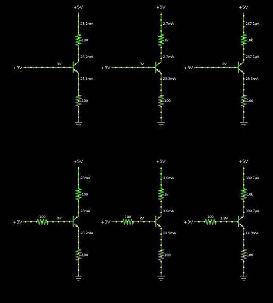
Before I tried to find the solution in sage the first time, I got stuck in that example as well. - Your way of replacing the transistor in the "saturation case" with a constant voltage source of 0.2 V between collector/emitter, and one of 0.6 V between base/emitter matches the "linear model" sheet I've posted earlier.
Before doing this, one assumes that the transistor is in linear/active mode, and solves the circuit always by replacing the transistor with constant current source of I
B * β. When V
CE < 0.2 V, the constant voltage source calcs above are used. - And for (calculated) I
B < 0 A it is in cut-off mode.
I know that this simplification is probably not accurate at all, but it is practical to use... I'd prefer some even simpler actually ;P
But somehow it doesn't show the picture anymore, so here it is again:
And the Ve equation for case 3
[tex]V_E = (\frac{Vin-Vbe}{R_B}+ \frac{Vcc - Vce(sat)}{R_C})* R_B||R_E||R_C[/tex]
Thanks again for solving those examples step by step!
The 1 / ( 1/R
B + 1/R
E + 1/R
C ) term just showed up in the equation (I don't see any physical reason for that - but there might be one by transforming the circuit somehow?), and it's a nicer way of writing it.
[tex]\frac{V_E}{100 Ω} = \frac{3V - (0.6 V + V_E) }{100 Ω} + \frac{5 V - (0.2 V + V_E)}{10 kΩ}[/tex]
[tex]V_E \frac{1}{100 Ω} + V_E \frac{1}{100 Ω} + V_E \frac{1}{10 kΩ} = \frac{2.4 V}{100 Ω} + \frac{4.8 V}{10 kΩ} = I_x[/tex]
[tex]V_E \frac{1}{R_B} + V_E \frac{1}{R_E} + V_E \frac{1}{R_C} = I_x[/tex]
[tex]V_E \frac{R_B + R_E + R_C}{R_B \cdot R_E \cdot R_C} = I_x[/tex]
[tex]V_E = I_x \frac{R_B \cdot R_E \cdot R_C}{R_B + R_E + R_C} = I_x \cdot R_B||R_E||R_C[/tex]
Most of the time yes, but as everything in electronics it's depend on a given circuit/application.
That's what I need to learn, this sense of knowing when to apply which rule of thumb... I'd like to understand the underlying physics too, but it's good to know when to do what.
Comparing it an everyday action, like opening a door... I don't calculate the exact force to apply to the door handle, and all the 3d transformations to move my hand etc. - Since we cannot see electro/magnetic fields and electric/magnetic flow, we have such a hard time getting that intuitive feel. Also we normally don't operate in the the megahertz and nano-pico regions... but I'm sure that it is possible to get a feel for analyzing/build electronic circuits. It's just the question of how to get there efficiently... ;) - Learning the math/physics. Applying it by building things, and *measuring*, adjust, *measure* adjust... I just made the experience with some basic BJT circuits I've built recently, that there's no point in just tweaking a circuit by changing resistor values for examples, when I don't understand what I'm doing. - Sure, one can "design"/tweak a circuit in the emulator or on the breadboard, and use it like that. But I just don't feel save by doing this. Trial'n'error is not the proper way of doing these things...
But in BJT we want high current gain so, the base current should be as small as possible. And Vbe voltage "sets" how much electrons is injected from emitter to base. But because the base is very thin the small number of electrons will recombine in the base. Also because the collector voltage is much larger then vbe this E field will sweeps those electrons into the collector (drift current due to large electric field (Vcc>>Vbe) ). So that almost all electrons that whose inject into emitter will reach collector terminal.
Yes, that makes sense... I cannot visualize the flow of electronics in the base correctly yet. But logically, it makes sense. The base/emitter depletion region is non-existing due to enough base/emitter voltage + emitter->base electron current, so that P-N junction looks almost like a short circuit (with a "constant" voltage drop). Electrons can now move form the emitter to the base. Now, to that electron current the whole transistor looks a bit like a reverse biased diode (P material of the base touching N region of the collector), with a "strong" depletion region in between. The difference to such a diode is, that the base emitter voltage makes the emitter current flow straight into that (physically thin) depletion region, so that the charge carriers can move over to the collector terminal... *trying to find the right picture to memorize*
