Question about majority and minority concentrations in diodes

  • Thread starter Thread starter theBEAST
  • Start date Start date
  • Tags Tags
    Diodes
AI Thread Summary
In a reverse-biased diode, the concentration of majority carriers (holes) increases near the junction due to the constant np product, where a decrease in electron concentration necessitates an increase in hole concentration. Despite the negative charge at the metal contact attracting holes, the electric field in the depletion region causes electrons to be swept away, leading to a pile-up of holes near the junction. This results in a reduced concentration of holes at the metal contact, which increases the potential barrier. Additionally, minority carrier concentrations increase near the junction as electrons are generated and move towards the n-side, leaving behind holes. Overall, the dynamics of carrier movement and recombination explain these concentration changes in both forward and reverse bias conditions.
theBEAST
Messages
361
Reaction score
0
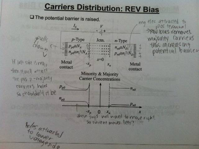
In my notes package it shows that for a REV biased diode, in the p type side, the concentration of majority carriers (pp0 holes) increases as we get closer to the junction. However, I don't get how this makes sense, since the metal contact between the negative terminal of the source and the p-type region is negatively charge, shouldn't we expect the holes to be attracted to the metal contact? Thus, in the graph shown below, the concentration of pp0 should be larger at the beginning and decrease as it gets closer to the junction?

PS: feel free to ignore some of the things I wrote :P
FSlj9LS.jpg
 
Engineering news on Phys.org
The np product at that point is given by n^{2}_{i}e^{F_n-F_p/kT}.

If none of these quantities could have changed at a given point, then it must be constant. As you see in the diagram the n_{p0} concentration drops to zero near the depletion region as those electrons have been are swept across by the large electric field.

So if the np product must be constant, and n decreases, p has to increase to account for it.

Conceptually, you could also think of holes being quickly swept from the other side and "piling up" at the end of the depletion region.
 
shallowbay said:
The np product at that point is given by n^{2}_{i}e^{F_n-F_p/kT}.

If none of these quantities could have changed at a given point, then it must be constant. As you see in the diagram the n_{p0} concentration drops to zero near the depletion region as those electrons have been are swept across by the large electric field.

So if the np product must be constant, and n decreases, p has to increase to account for it.

Conceptually, you could also think of holes being quickly swept from the other side and "piling up" at the end of the depletion region.

Hmm, that makes a lot of sense when you put it that way. But what about the other way to think of it? The fact that there is a negative charge on the left contact and thus the positive holes should be attracted to it. This should result in an increase in concentration of holes near the metal contact. In other words, there are less holes close to the pn junction and thus the potential barrier is increased?


Also, can anyone explain this then:
5zbPAcH.png


Why would the minority concentrations increase near the junction?
 
Last edited:
Hmm, that makes a lot of sense when you put it that way. But what about the other way to think of it? The fact that there is a negative charge on the left contact and thus the positive holes should be attracted to it. This should result in an increase in concentration of holes near the metal contact. In other words, there are less holes close to the pn junction and thus the potential barrier is increased?Also, can anyone explain this then:Why would the minority concentrations increase near the junction?
Look first of all, holes can't really do anything even if they are attracted by terminal. Look it the other way, its the electrons that move and generate holes. Now having said that first look at the frwd bias condition.

Now we know that the depletion region is formed of two polarities of atoms negative and positive. The positive atom or the donor exists on the N side and negative atom exists on the P side.
Now as we forwards bias the PN junction the free electrons on the N side will penetrate the depletion region and impart energy to the immobile positive atoms to release an electron, this way a hole will be created together with an electron. As holes don't really move the electron will move towards the P side whereas the hole will be left behind thus reducing the depletion region.

Same will happen on the P side, some of the incoming electrons will collide with the negative immobile atom and this will eject an electron from the atom thus creating a hole and electron simultaneously, thus reducing the junction width.

As we move towards the metal contact in P side the hole concentration will become constant whereas the excess electron concentration will also become constant after recombination as electron hole pairs are created in pairs.

Same applies for the reverse bias as a free electron on P side strikes the immobile negative atom a electron and hole will be generated simultaneously and this accounts for the decreased concentration of electrons and increased concentration of holes as electrons generated will move towards the N side leaving the hole.
 
Last edited:
While I was rolling out a shielded cable, a though came to my mind - what happens to the current flow in the cable if there came a short between the wire and the shield in both ends of the cable? For simplicity, lets assume a 1-wire copper wire wrapped in an aluminum shield. The wire and the shield has the same cross section area. There are insulating material between them, and in both ends there is a short between them. My first thought, the total resistance of the cable would be reduced...
Hi all I have some confusion about piezoelectrical sensors combination. If i have three acoustic piezoelectrical sensors (with same receive sensitivity in dB ref V/1uPa) placed at specific distance, these sensors receive acoustic signal from a sound source placed at far field distance (Plane Wave) and from broadside. I receive output of these sensors through individual preamplifiers, add them through hardware like summer circuit adder or in software after digitization and in this way got an...
I am not an electrical engineering student, but a lowly apprentice electrician. I learn both on the job and also take classes for my apprenticeship. I recently wired my first transformer and I understand that the neutral and ground are bonded together in the transformer or in the service. What I don't understand is, if the neutral is a current carrying conductor, which is then bonded to the ground conductor, why does current only flow back to its source and not on the ground path...
Back
Top