Solving 555 Based Switcher Challenge for Niхie Clock

  • Thread starter Borek
  • Start date
In summary: Comparator and voltage reference are a great way to keep the output voltage stable even when the load changes.
  • #1
Borek
Mentor
28,951
4,245
(in a way this is a continuation of the previous thread on the solution choosing strategy)

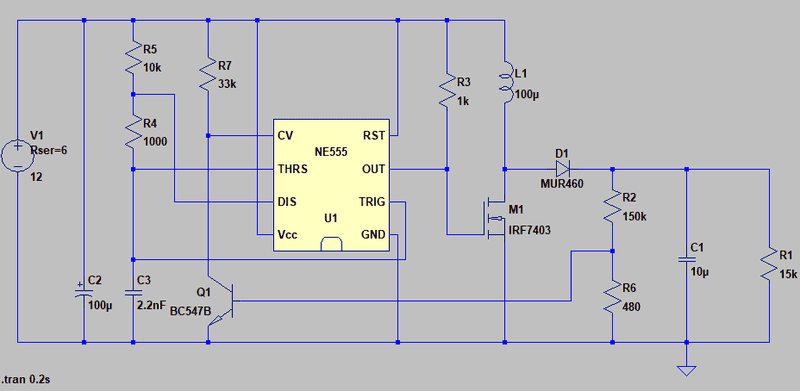
So, I needed DC-DC switcher, capable of delivering up to 200 V and 10 mA. Idea is simple - coil, interrupting the current, "collecting" the voltage. Easy to implement with 555, but difficult to control the output voltage with just frequency and duty cycle of oscillations. Some googling (this is switcher for a Niхie clock and I am not a first one to build it) yields this solution (element values can be different and actually R6 is a potentiometer allowing to control the voltage on the load R1):
SPS555.png


What I don't like about it is that the output voltage depends on both the V1 voltage and R1 resistance. But I liked the idea of using CV (AKA CON) to change the duty cycle, so I decided to try a bit different approach, with a voltage reference and comparator:
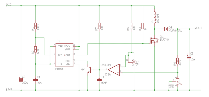
SPS555_with_a_comparator.png


In theory VOUT should not depend on the load nor VCC. I tested a very similar circuit in the LTSpice:
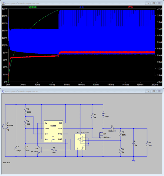
SPS_LTSpice_simulation.png


(it is not identical to the one I build as I couldn't find LTSpice models for LM393N comparator nor KA431LZ voltage reference, so I used a functionally equivalent chip from the program library). Green - voltage on the load (VOUT), red - current drawn from V1, blue - current through L1.

Long story short - it works not only in the simulation, but also on a breadboard. I have built a prototype and it powers my clock right now. No elements get hot, voltage looks stable (it is at 162 V now, and floats by about ±0.2), it does change a bit with load and VCC, but I have not yet tested it too heavily to see by how much.

Comments welcome.

(sorry, looks like PF resized pictures, I hope they will be readable)
 
Engineering news on Phys.org
  • #2
How quickly can the load presented by the clock display change? One key to verifying switcher design is to present worst-case AC loads to the regulation and compensation circuit. I'm guessing that the display load won't change more than 1/sec or 10/sec, right? Probably the compensation can keep up with that. What is your switching frequency?
 
  • #3
This is a four digit clock so the load changes just once per minute (I have no more Niхie tubes, these are large ones, rather expensive). 555 works at about 35 kHz (can't remember precisely). Initially I tried 1 μF C3 and the simulated output voltage was oscillating, so I replaced C3 with much larger one (that in turn means it takes about 0.1 sec to get to the desired voltage, but I don't think it is a problem).
 
  • #4
Glad you got something up and running. I would recommend a diode across the power supply. Specifically from the top side of L1 to ground. This prevents developing a reverse polarity from occurring in the event of losing the low voltage supply. C2 should help prevent this but just to be safe I would put a diode in. I would also add some power supply bypassing capacitors physically very close to the top side of L1 and the GND node on the MOSFET. When the switching occurs you want as short as possible leads to good low ESR/ESL capacitors.
 
  • #5
Thank you for your comments.

Averagesupernova said:
I would recommend a diode across the power supply. Specifically from the top side of L1 to ground.

That's what you mean, right? Not exactly across the power supply, but it was convenient to put in on the schematics close to L1, to keep things close to your description.

diode_added.png


I understand it is one of those things you add "just in case" - rarely needed in reality, but a good practice to stay on the safe side?

I would also add some power supply bypassing capacitors physically very close to the top side of L1 and the GND node on the MOSFET.

Can you elaborate? Apparently either my English or my understanding of circuits (probably both) fails me as I am not sure where to put these capacitors. I understand the general idea of adding C to smooth out the ripples, I just don't understand where to put it in the case of the MOSFET (the L1 one should be in parallel to the just added diode, right?). And we are talking about 100 nF, just like the ones typically added around ICs?

Should I add another 100 nF capacitor near the 555? That's what I intended to do at first, but as there is a large C2 (intended to help supply the high current for L1, the 12V power supply that runs whole clock is rated 1A) I thought it might be not necessary. Edit: after some more thinking yes, I should.

And any comments on the general idea of using comparator and voltage reference in such cases?
 
Last edited:
  • #6
Hello again Borek. Some folks would consider power supply bypassing capacitors to be a black art. When you stop and think about though, what is really happening is that the copper traces on circuit boards are actually small inductors. This is of little consequence at lower frequencies. But as the frequencies involved increase this inductance can become significant. Granted that 35 khz may not be a very high switching frequency but it will likely contain a lot of harmonics.
-
Add the cap or caps in parallel with the diode that you added. When you place appropriate bypass capacitors physically very close the the inductor and MOSFET on your circuit board you no longer have the effects of the longer circuit board traces acting as inductors.
-
In the past I have found digikey will have a nice guide in power supply bypass capacitors selection. I realize you may not order your parts from the USA but you can certainly exploit their website to select appropriate parts. www.digikey.com.
-
Keep in mind that the 100 uF cap you have may not look like a cap at frequencies that are harmonics of 35 khz. My rule of thumb would be to use a bypass capacitor or even several directly across the 555 as well.
 
  • Like
Likes Borek
  • #7
Sigh, the switcher worked perfectly well up to today (almost three weeks) - in the meantime I checked the temperature of elements several times, they were not even warm. Today while I started working on PCB to make a final, soldered version I smelled something burning - took me a moment to find out it was the MOSFET that got so hot it burned hole in the breadboard.

What would be your guess - problem with design, or I was just unlucky: the element was faulty, or some contact got oxidized and warmed up? MOSFET was switching currents in 1A range, so I can imagine some kind of a thermal runaway.
 
  • #8
I thought I smelled something...

Can you post your final circuit and final control loop values? What load were you running with when the smoke got let out? Any chance you touched part of the circuit while it was running and caused EOS and latchup (not likely with a power circuit, but just asking)?
 
  • #9
Untitled-1.png


I am not sure what you mean by control loop values - R11 was tuned so that the CON was grounded through Q2 and switching the 555 cycle off when the VHIGH was 162 V.

The load @162 V was more or less the same all the time - in the 10 mA range (unless something strange happened, but the Nixie lamps, which are on another PCB are OK so it is rather unlikely they were source of the problem). The only large current is the one going through L1 and Q1.

The breadboard was powered with two ±4 inch wires screwed to a Degson type terminal residing on another PCB with RTC, ATmega microcontroller and several other elements (this PCB is attached directly to the 12 V power supply). I moved the PCB several times checking some details. I don't think I touched the breadboard, but it was definitely moved/rocked about an hour or two before it burned. I have moved it earlier as well though, without any problems.
 

Attachments

  • Untitled-1.png
    Untitled-1.png
    13.3 KB · Views: 514
  • #10
Hmm... sending smoke signals, must have been in major distress.

There is a good chance that L1 is also destroyed, so you might as well order another if you don't have a spare.

Here is a detailed troubleshooting approach that may seem the wrong way around in spots. The specific sequence is intended to elicit as much information as possible about the root cause of failure without causing further damage. To track down the cause, please report the results of all these tests that you run; and anything else you may notice that gets your attention or are not sure of. Details matter in troubleshooting!

First a few recommendations. Either of the first two could be the underlying culprit:
1) R10 should be 1/2W due to voltage limitation of physically smaller resistors
2) C5 should be at least 250V
3) Add a 0.47μF, 250V metallized film capacitor across C5

The trouble was probably a loose connection somewhere, but here are some other possibles I can come up with at the moment are:
1) Defective Q1
2) Loose connection in Q1 gate circuit
3) Failure or loose connection in 555 circuit
4) Failure or loose connection in feedback circuit
5) Short circuit or overload on output
6) Q1 itself was oscillatingAt this point Q1 is obviously defunct so gently remove it from the circuit. Gently because we don't want to disturb other evidence. An approach to " gently" could be disconnect either end of the inductor AND either end of D1. Now use whatever means you have (hopefully a 'scope) to check that the 555 is oscillating, it should be.

Check for oscillation at the 555 timing components (pin 2, 6, or 7).
  • If no oscillation at the timing RC components
    • verify approx. 8V±10% at 555 pin 5.
      • If not ≅8V, disconnect Q2-Collector and check for oscillation again.
        • If oscillation, troubleshoot Q1 and Op-Amp circuit.
        • If no oscillation, replace 555 and verify there is oscillation.
      • Reconnect Q2-C and verify oscillation
  • If there IS oscillation at the timing RC components
    • Check oscillation at the 555 Output (pin 3), it should should swing between 0.25V and +12V (supply voltage.)
      • If there is little or no signal at 555 pin 3
        • Gently disconnect Q1 Source from Gnd
        • Check oscillation at the 555 Output (pin 3)
          • If present, check oscillation at Q1 Gate
          • If absent or low level, either 555 is faulty or there is an open connection around 555, R3, Q1-G
Replace Q1.

For initial testing, L1 can be replaced with a 470Ω, 1/2W resistor. This will allow safe testing for intermittents from parts of the feedback loop, the 555, and Q1. There won't be any output, so monitor Q1 Drain voltage.
If you can inject a controllable voltage at the R10-R11 junction you can also test the OpAmp, reference voltage, and Q2.

If you have a 'scope, check Q1 Drain for high frequency oscillation. It may appear as some fuzziness on the transitions of the switching signal or at the high or low voltage levels. If there is any high frequency stuff on the transitions, try putting a low value resistor (10Ω - 100Ω) in series with the Gate of Q1. This must be done with the shortest practical lead length between the resistor and Q1. Find the lowest resistance that stops the high frequency stuff then use a value 15% to 30% higher.

If there is high frequency stuff on the high or low voltage levels it means the gate bias is not swinging enough to respectively turn off or turn on Q1. I'll let you figure that one out!

Reconnect D1.
Once again, check for high frequency oscillation of Q1.

Remove the 470Ω resistor at Q1 Drain and install new L1.
Cross your fingers and see if it works.
 
  • Like
Likes jim mcnamara and jim hardy
  • #11
Two one-cent thoughts here:
1. In my limited experience with home-brew SMPS
inductance of interconnecting wires was troublesome.
At your low current it shouldn't be as bad,
but take a look at the wires through which your switched currents flow with an eye toward minimizing their inductance.
Borek's555switcher.jpg


2. I've had lots of trouble using fast comparators - they'll oscillate when changing state.
Here's a precaution from the TI datasheet at http://www.ti.com/lit/ds/symlink/lm393.pdf

upload_2017-10-26_12-16-33.png


Observe with 'scope the output of your LM393 ? Is it changing state decisively ?
If transitions aren't snappy and clean, a teeny bit of hysteresis might help .
A megohm or so between pins 1 and 3 ? Start higher and iterate toward value that gives clean switching but not excessive ripple in your high voltage .

......

And at two cents for that advice, I'm overpriced .

old jim
 

Attachments

  • Borek's555switcher.jpg
    Borek's555switcher.jpg
    23.1 KB · Views: 523
  • upload_2017-10-26_12-16-33.png
    upload_2017-10-26_12-16-33.png
    30.5 KB · Views: 494
  • Like
Likes Tom.G
  • #12
  • Like
Likes Averagesupernova
  • #13
One more observation ( academic interest only ) about that comparator

Borek's555switcher2.jpg


Working from a schematic it looks like positive feedback which is usually means trouble. But how your wires are physically routed determines whether that's really so.
Furthemore,
in your case i think that might well provide the positive feedback hysteresis loop this circuit needs albeit not quite instantaneously.

When you close a control loop by adding feedback all sorts of new possible behaviors suddenly appear... because what was just forward gain G becomes closed loop gain G/(1+GHfeedback) ,
i.e. a denominator appears
and if that denominator can be made zero you can rest assured playful Mother Nature will do so.

Figuring out closed loop troubles is a lot of fun..

I'm enjoying your adventure - thanks for sharing !

old jim
 

Attachments

  • Borek's555switcher2.jpg
    Borek's555switcher2.jpg
    12 KB · Views: 477
Last edited:
  • #14
Please note: it was a mess of wires on the breadboard prototype, so discussing possible problems with incorrect design of wiring is IMHO a moot at the moment (and no way to make it fit 5 square centimeters).

I will dive deeper in the next days, but just to give you a better impression of what have happened:

IMG_8514.jpg


I wonder if the black plastic between MOSFET's source (leftmost leg on the picture) and the ground connector doesn't show where things went wrong.

Does 35 kHz already count as a high frequency in this context?
 

Attachments

  • IMG_8514.jpg
    IMG_8514.jpg
    62.5 KB · Views: 467
  • Like
Likes donpacino
  • #15
Borek said:
MOSFET was switching currents in 1A range, so I can imagine some kind of a thermal runaway.

I might be mistaken, but I don't think solderless bread boards are rating for more than 1 A. 1 A will be pushing the limits at best.

Also with solderless breadboards, you add a few pF of capacitance between the components in any given row. That is something you may want to add to your simulation, just to see the effects.
 
  • #16
You can try using multiple fets to improve heat dissipation and lower the current through each breadboard leg?
 
  • #17
I can't tell
but here at 300% the base side lead of R9 looks awfully close to the metal tab, which i think is connected to drain?
If so and they touch , well,,,
upload_2017-10-26_16-5-58.png
 

Attachments

  • upload_2017-10-26_16-5-58.png
    upload_2017-10-26_16-5-58.png
    62.2 KB · Views: 435
  • #18
No, it is just a perspective trick. Resistor is several millimeters behind and in a much lower position, even if forced to touch it will touch the ceramics, not the metal.
 
  • Like
Likes jim hardy
  • #19
Borek said:
No, it is just a perspective trick.

And what a difference ambient room light makes !
In daylight i couldn't see that the wire went behind the MOSFET ,
and i mistook this little line for it.
Sorry for the silly mistake. Quite plain now that sun is down.
Time to dust off the screen i think.
upload_2017-10-26_22-14-58.png
 

Attachments

  • upload_2017-10-26_22-14-58.png
    upload_2017-10-26_22-14-58.png
    35.9 KB · Views: 463
  • #20
IMHO, I would see that as a result of a high(er) resistance connection that was stressed after Q1 shorted.

Borek said:
img_8514-jpg.jpg


I wonder if the black plastic between MOSFET's source (leftmost leg on the picture) and the ground connector doesn't show where things went wrong.
 

Attachments

  • img_8514-jpg.jpg
    img_8514-jpg.jpg
    62.5 KB · Views: 458
  • Like
Likes jim hardy
  • #21
I will throw in my 2 cents. Something no one has mentioned at all is that a 555 used in this manner does not really change the duty cycle when the voltage on pin 5 is moved around. The frequency is changed. In this particular setup as the output voltage rises above the reference voltage, the transistor will turn on causing the voltage to drop on pin 5 which raises the frequency of the free running 555. That is not to say that you cannot obtain some regulation by bumping the frequency around, but it is not changing the duty cycle. So the question is, when this was up and running, what was the voltage on pin 5? Was it so low that there was a possibility that the free running oscillator stopped and simply turned on the MOSFET and caused the evident meltdown?
-
Edit:
I had ASSUMED that IC 5 was an opamp, but rereading I see it is a comparator. That doesn't seem right to me. Isn't that part of a voltage regulating circuit normally supposed to be an error amplifier?
 
  • #22
Averagesupernova said:
I will throw in my 2 cents. Something no one has mentioned at all is that a 555 used in this manner does not really change the duty cycle when the voltage on pin 5 is moved around. The frequency is changed. In this particular setup as the output voltage rises above the reference voltage, the transistor will turn on causing the voltage to drop on pin 5 which raises the frequency of the free running 555. That is not to say that you cannot obtain some regulation by bumping the frequency around, but it is not changing the duty cycle. So the question is, when this was up and running, what was the voltage on pin 5? Was it so low that there was a possibility that the free running oscillator stopped and simply turned on the MOSFET and caused the evident meltdown?
-
Edit:
I had ASSUMED that IC 5 was an opamp, but rereading I see it is a comparator. That doesn't seem right to me. Isn't that part of a voltage regulating circuit normally supposed to be an error amplifier?
Good question. Bang - Bang control perhaps? There is enough output filtering to make that viable. Guess we'll just have to wait for the repairs and see what it does.
 
  • #23
Averagesupernova said:
Something no one has mentioned at all is that a 555 used in this manner does not really change the duty cycle when the voltage on pin 5 is moved around. The frequency is changed.

I can't check the real thing for obvious reasons, what I have is the LTSpice simulation (slightly different circuit, but with exactly the same internal logic, voltage reference and voltage comparator used to control CONT; red is the voltage on the 555's output pin, blue is the voltage on the C5, green is the L1 current):

Untitled-3.png


Initially 555 oscillates all the time, once the voltage on the C5 gets high enough high current through L1 is switched on only when necessary (it does oscillate in the tens of mA range). My understanding is that fine tuning the frequency and duty cycle is important to get as high efficiency as possible, and I selected them to minimize the initial time required for the voltage on C5 to rise up to 200 V. Once the circuit is there for most of the time MOSFET is off and the oscillations are on only when needed (perhaps their parameters are not optimal, but they were good enough to keep the output voltage high).

Averagesupernova said:
So the question is, when this was up and running, what was the voltage on pin 5? Was it so low that there was a possibility that the free running oscillator stopped and simply turned on the MOSFET and caused the evident meltdown?

I am not sure I understand. Do you mean the oscillator can stop in the "on" state, with high voltage on the output pin, despite CONTROL voltage (pin 5) being lower than the TRESHOLD voltage?

LTSpice simulation shows voltage on CONTROL to be just zero when the voltage on C5 is high enough.
 

Attachments

  • Untitled-3.png
    Untitled-3.png
    8.4 KB · Views: 390
  • #24
Tom.G said:
Bang - Bang control perhaps?

Clearly.
Comparator output high clamps Control pin to ground . That should stop oscillation because voltage at THRESH is > 2/3 the zero volts at CON.

upload_2017-10-27_8-12-0.png


Well, at first it is anyway.
Then we have competition between two transistors
Q2 pulling CONTROL low
and the 555's internal DIS transistor pulling THRESH and TRIG both low,
and since TRIG can override THRESH
it might make possible this scenario - i honestly don't know.
Borek said:
Do you mean the oscillator can stop in the "on" state, with high voltage on the output pin, despite CONTROL voltage (pin 5) being lower than the TRESHOLD voltage?
.
2/3 of zero is not greater than 1/3 of zero, so if both CON and TRIG/THRESH(which are tied together) really make it to zero
it looks to me like the 555 might oscillate - TRIG below 1/3 of zero would release DISCH , which within microseconds let's TRIG/THRESH rise above 2/3 of zero, again asserting DISCH .

Might that be what is this hash on L1 current ? (a snip at 400%)
upload_2017-10-27_8-28-24.png


I don't know.

But i don't see any mechanism for constant high aside from R7 falling out of the breadboard.

old jim
 

Attachments

  • upload_2017-10-27_8-12-0.png
    upload_2017-10-27_8-12-0.png
    5.1 KB · Views: 452
  • upload_2017-10-27_8-28-24.png
    upload_2017-10-27_8-28-24.png
    334 bytes · Views: 391
  • Like
Likes Tom.G
  • #25
To me, pulling the control pin to zero is running the device in undefined territory. If gated oscillations is what we are after then use the reset pin.
-
Also, I would add some positive feedback on that comparator.
 
  • Like
Likes jim hardy
  • #26
Averagesupernova said:
To me, pulling the control pin to zero is running the device in undefined territory.

I agree with that. I searched TI datasheet for advice on minimum Vcontrol for reliable operation to no avail.
 
  • #27
Old Signetics 555 timer datasheet is here, it's way more informative.

https://ia802706.us.archive.org/35/items/Signetics555556Timers/Signetics555556Timers.pdf

DISCH pin can probably pull TRIG and THRESH to around 0.1 volt
Don't know what is Vcesat for Borek's Q2, and i don't know how close to GND those comparator inputs will operate.

You're right i think - RESET might be a better way to stop oscillation.
from page 9 of old Signetics:
upload_2017-10-27_9-25-34.png


pull it below 0.4V.
 

Attachments

  • upload_2017-10-27_9-25-34.png
    upload_2017-10-27_9-25-34.png
    30.6 KB · Views: 390
  • Like
Likes donpacino
  • #28
Averagesupernova said:
To me, pulling the control pin to zero is running the device in undefined territory.

I am in an undefined territory since I started playing with electronics last year. Actually I am often quite happy if I understand 50% of what you all write :nb)

If gated oscillations is what we are after then use the reset pin.

I believe I tried and it worked, I decided to use CONT pin as that was solution used in another 555 based switcher I have here (one that is quite popular between those playing with Niхiе clocks). As nobody pointed out any obvious flaws in the idea when I posted the schematic for the first time, I assumed it was not completely off.
 
  • #29
Borek said:
I am in an undefined territory since I started playing with electronics last year. Actually I am often quite happy if I understand 50% of what you all write :nb)

Let people know if you don't understand, and they can prob give you a simpler explanation.
 
  • #30
I am doing my best
to not be a pest :wink:
 
  • #31
Borek said:
I am doing my best
to not be a pest :wink:
I'm guessing many of us are on here because we genuinely enjoy helping people solve problems.

Ask a question, bring us joy haha
 
  • Like
Likes jim hardy
  • #32
Borek said:
I am doing my best
to not be a pest :wink:
I'm the pest. Look at all the vicarious experimentation i do here !

There's an old metaphor - like the midget in a nudist colony my nose gets in everybody's business I'm sensitive about meddling too much.

Thanks for tolerating me.

old jim

PS you're doing GREAT at electronics.
 
  • #33
I have never liked doing very much to the control pin. It is ok to dial it around some but even those schematics that do not use a comparator and still have a transistor have the potential to pull that pin a lot lower than it should be.
-
Consider this: As the voltage on the control pin gets quite low, the frequency of oscillation will become relatively high. This causes a lot more transitions between low and high. We know the slew rate is never perfect so the MOSFET spends more time in transition, neither fully on or fully off. This means more heat.
-
Ideally I think the best way is to have a fixed frequency and vary the duty cycle. Gated oscillation will work fine too though.
 
  • #34
If any of you remember cameras that had Xenon flashtubes, you may recall the inverters going up in frequency as the high voltage cap charged. When the cap reached desired voltage, the inverter changed to Bang - Bang mode to keep it charged. This is exactly what the simulator trace shows with Boreks circuit.
Borek said:
untitled-3-png.png
jim hardy said:
Might that be what is this hash on L1 current ? (a snip at 400%)
upload_2017-10-27_8-28-24-png.png
Probably L1 ringing with stray capacitance.
 

Attachments

  • untitled-3-png.png
    untitled-3-png.png
    8.4 KB · Views: 328
  • upload_2017-10-27_8-28-24-png.png
    upload_2017-10-27_8-28-24-png.png
    334 bytes · Views: 325
  • #35
Averagesupernova said:
To me, pulling the control pin to zero is running the device in undefined territory.

From page 16 (11 of the pdf) of that old Signetics 555 datasheet at
https://ia802706.us.archive.org/35/items/Signetics555556Timers/Signetics555556Timers.pdf
upload_2017-10-27_20-55-40.png


Driving CON to zero indeed looks risky .
 

Attachments

  • upload_2017-10-27_20-55-40.png
    upload_2017-10-27_20-55-40.png
    31.8 KB · Views: 343

Similar threads

  • Electrical Engineering
Replies
14
Views
813
  • Electrical Engineering
Replies
10
Views
1K
  • Electrical Engineering
Replies
10
Views
2K
  • Electrical Engineering
Replies
17
Views
2K
Replies
7
Views
2K
Replies
1
Views
965
  • Electrical Engineering
Replies
14
Views
6K
Replies
1
Views
2K
Replies
4
Views
3K
  • Electrical Engineering
Replies
24
Views
8K
Back
Top