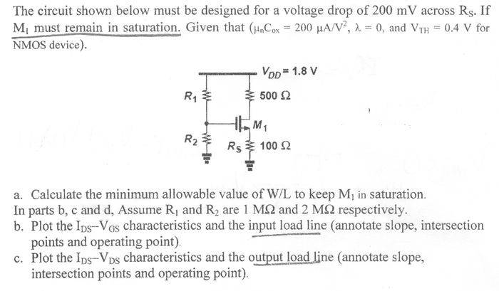
What is the significance of input and output load lines in microelectronics?

Join the discussion
Registration is free. Start your own thread to ask a follow-up.
2 replies · 2K views
Ahmad Kishki
Messages
158
Reaction score
13
Homework Statement
o88fyYJ.jpg


I am not sure i know what is meant by the input load line and the output load line in parts b and c. I tried looking it up in my book (fundamentals of microelectronics by razavi) but to no avail. Any help is appreciated.
 
Physics news on Phys.org
To derive the output load line imagine removing everything from the circuit except the RD and RS resistors, then plotting I vs. V where I is the current in those resistors and V is the voltage across the "empty gap" between them. It is immaterial what element you insert into that gap, the current through it and voltage across it are fully constrained by that pair of resistors together with the supply voltage, and this gap's I vs. V plot is known as the output DC load line.
 
  • Like
Likes   Reactions: Ahmad Kishki
* Input load line:
VGS=VG-VS=VG-IDS*RS.
From this: IDS=VG/RS-VGS/RS.
This gives a straight line crossing the IDS=f(VGS) graph in one point.

* Output load line
VDS=VD-VS=VDD-IDS*RD-IDS*RS=VDD-IDS*(RD+RS).
From this: IDS=(VDD-VDS)/(RD+RS)=VDD/(RD+RS)-VDS/(RD+RS).
This load line has a negative slope.
 
  • Like
Likes   Reactions: Ahmad Kishki