NPN BJT transistor: base voltage / emitter current

In summary: When you look at the various graphs in datasheets and online, you may not see how the different values depend on each other. This is because the graphs are typically for "linear" operation (i.e. within the "active region"). However, when the transistor is "not in its active region", the relationship between Ic and B no longer holds. In order to understand how the different values depend on each other, you would need to recalculate the voltages Vce across the transistor.
  • #1
1rel
43
3
I don't know how to calculate the voltages at the bases of every transistor shown in the lower row of that picture (~3V (2.9..V), ~2V, ~1.8V). Any help would be appreciated! - I'm currently trying to figure that out...
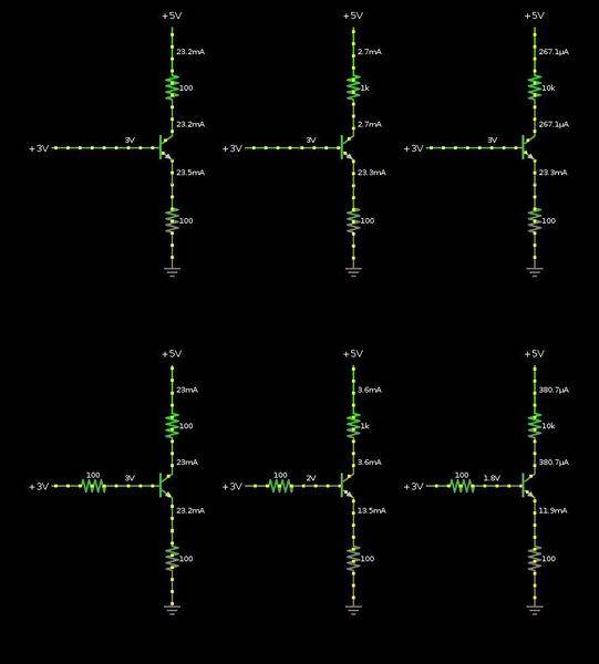
Screenshot_2016-07-08_22-12-56.jpe


The other thing I don't really understand: Why do the transistors in the upper row all have an equal emitter current? Does the the collector-emitter current really only depend on the base current (Ice = Ib * hfe), and not on what's in front of the collector (100 Ohm, 1 kOhm, 10 kOhm)? And why can transistors do this?

(I'm currently trying to learn more about the absolute basics in electronics. - The used simulation tool can be found here. The goal is to understand things like current mirrors and differential amplifiers... but I don't even really get how a simple transistor (BJT) works. Oh well.)
 
Engineering news on Phys.org
  • #2
In the upper row you keep the base voltage constant at +3V. This means that the emitter voltage must be Vbe below +3V or about 2.3V. 2.3V divided by 100Ω (Re) equals 23mA.

In the lower row, the base is not kept at a constant voltage, but at +3V - Rb⋅Ib. Now, Ib depends on Ic and the current gain of the transistor - and Ie = Ic+Ib...
 
  • Like
Likes 1rel
  • #3
1rel said:
The other thing I don't really understand: Why do the transistors in the upper row all have an equal emitter current? Does the the collector-emitter current really only depend on the base current (Ice = Ib * hfe), and not on what's in front of the collector (100 Ohm, 1 kOhm, 10 kOhm)? And why can transistors do this?

Keep in mind that the transistor acts as a voltage-controlled current source (Vbe controls Ic).
This is in accordance with the well-known Shockley-equation: Ic=Is*exp(Vbe/Vt -1) with Vt=temperature voltage (app. 26mV at room temp). The base current Ib is always a small (fixed) portion of the collector current Ib=Ic/B.

That means: It does not matter if the collector resistor Rc is 1k or 10k - the transistor always produces the same current Ic.
However, this applies only as long as the transistor is operated within its active region.
That means: The collector-emitter voltage Vce must not fall below app. 1V.
Otherwise, the transistor is not operated anymore within its "linear" region - and the relationship Ib=Ic/B does not apply.
Therefore: To understand the voltages and currents in the given examples, I recommend to recalculate the various voltages Vce across the transistor. This can be done simply by applying Ohms law for the the collector as well as emitter resistors.

(Note: The above description is the idealized case; in reality, there is a small dependence on Rc resp. Vce because the transistor is, of course, not an IDEAL current source. But this effect is not considered in all transistor models).
 
Last edited:
  • Like
Likes 1rel
  • #4
Thank you for the help!

Svein said:
In the upper row you keep the base voltage constant at +3V. This means that the emitter voltage must be Vbe below +3V or about 2.3V. 2.3V divided by 100Ω (Re) equals 23mA.

Yes, that makes sense!

At the 3 configurations in the top row:
Assuming that the transistor is in its "active region" or even more so in saturation, the collector-emitter voltage drop is small, and the collector-emitter path can be regarded to be a short circuit (right?). So, I can apply Ohm's Law to calculate the currents through the Rc resistors:

(Vcc = 5V and Ve = 5 V - 2.3 V = 2.7 V):
For Rc = 1 kΩ : Ic = ( Vcc - Ve ) / Rc = 2.7 V / 1 kΩ = 2.7 mA
For Rc = 10 kΩ: Ic = ( Vcc - Ve ) / Rc = 2.7 V / 10 kΩ = 270 μA

This seems to coincide with the values shown in the simulation...

But when the transistor is at the edge of becoming active (low base current?), it has a higher resistance on the collector-emitter path and the calcs above don't work anymore.

The simulation shows a collector current Ic of 23.2 mA. So the Rec of the transistor could be calculated like this I guess:

For Rc = 100 Ω and given Ic = 23.2 mA (sim):
Vc = Vcc - Ic⋅Re ) = 5 V - 23.2 mA ⋅ 100 Ω = 2.68 V
(((Rce = Vc / Ic = 2.68 V / 23.2 mA ≈ 116 Ω)))
EDIT: Rce = Vc / Ic - Re = 2.68 V / 23.2 mA - 100 Ω ≈ 16 Ω

How can I really understand this? When I look at the various graphs in datasheets and online I often don't really see how the different values depend on each other, and which value to pick to start the calculation of the values in a given circuit (even as simple as the one above :S). For example, I always thought that the base current is much smaller than the controlled collector/emitter current. But it is not true... It seems like the base/emitter voltage difference is always the same (1 diode drop ≈ 0.6V), and the base voltage somehow controls the SUM of the base-emitter/collector-emitter currents (LvW: yes, a voltage controlled current source. I answer later on that)... So the base current can be in fact much larger than the collector current... hm. I need to work on my model...
Svein said:
In the lower row, the base is not kept at a constant voltage, but at +3V - Rb⋅Ib. Now, Ib depends on Ic and the current gain of the transistor - and Ie = Ic+Ib...

Yes, but I don't really get that yet. I'm trying to figure out how to calculate these values first on paper first, and later hopefully understand the transistor model more intuitively... Probably I build this up on the bread board today.

BTW: The current gain of the simulation transistor model is fixed at 100, which makes it easier to understand the numbers. BTW, here is the simulation file used, now correctly linked (geat simulator by the way with lots of instructive examples)
More later...
 
Last edited:
  • #5
1rel, regarding the lower row:
When the transistor is in its active region (lower row, most left circuit), what is the voltage drop across the base resistor caused by the base current (when the current gain is 100)? Is there any severe difference when compared with the most left circuit in the upper row?
 
  • Like
Likes 1rel
  • #6
Where is your problem in understanding the load line concept?
* The transitor data sheet contains a set of characteristic curves Ic=f(Vce) with parameter Ib or Vbe (in your case: Ib).
* However, due to the rising voltage drops across Rc and Re (for rising current Ic), the remaining voltage for Vce decreases correspondingly.
That means: You cannot have any combination (Ic,Vce) as suggested by the data sheet curves.
That is the meaning of the load line: It shows (crossing points) which combinations (Ic,Vce)are possible for fixed resistors and a fixed supply voltage.
 
  • Like
Likes 1rel
  • #7
LvW said:
1rel, regarding the lower row:
When the transistor is in its active region (lower row, most left circuit), what is the voltage drop across the base resistor caused by the base current (when the current gain is 100)? Is there any severe difference when compared with the most left circuit in the upper row?

Things I can write down after looking at the circuit in the lower row, and convert it to the "linear mode" replacement circuit (see above), I can write down those things about it:

(1) VIN = RB ⋅ IB + VBE + RE ⋅ IE
(2) IC = β ⋅ IB
(3) IE = IC + IB = IB ⋅ (1+β)
(4) VCC = VRC + VCE + VRE
(5) VRC = RC ⋅ IC
(6) VRB = RB ⋅ IB
(7) VRE = RE ⋅ IE
(8) VC = VCC - VRC
(9) VB = VIN - VRB
(10) VE = VB - VBE
(11) VCE = VC - VE
(12) VBE = 0.65 V
(13) β = 100
(14) VIN =3 V
(15) VCC = 5 VIB = ( VIN - VBE ) / ( RB + RE * ( 1 + β ))
VCE = ( VCC - IB * ( 1 + β ) * RC ) - RC * β * IB
VB = VIN - RB ⋅ IB
IC = β ⋅ IB
VC = VCC - RC * IC
VE = VB - VBE
IE = IC + IB
VCE_check = VC - VEAnd get:

RC = 100 Ω, RB = 100 Ω, RE = 100 Ω (lower row, left)
VCE ≈ 0.369 V > 0.2 V
IB ≈ 230 μA > 0.0 A
IC ≈ 23.0 mA
IE ≈ 23.3 mA
VC ≈ 2.70 V
VB ≈ 2.98 V
VE ≈ 2.33 V

That seems to be about equal to the values in the simulation.

But for the other circuits in the lower row, I get negative VCE, so they are in saturation... and I'm still trying to figure out the numbers in the "saturation model" from above...
 
Last edited:
  • #8
LvW said:
Where is your problem in understanding the load line concept?
* The transitor data sheet contains a set of characteristic curves Ic=f(Vce) with parameter Ib or Vbe (in your case: Ib).
* However, due to the rising voltage drops across Rc and Re (for rising current Ic), the remaining voltage for Vce decreases correspondingly.
That means: You cannot have any combination (Ic,Vce) as suggested by the data sheet curves.
That is the meaning of the load line: It shows (crossing points) which combinations (Ic,Vce)are possible for fixed resistors and a fixed supply voltage.

Thank you for the patience :) Yes, I more or less see that, and also tried to play through an example with a resistor and a diode, and a 2 resistors in series. It works -- the crossing points show the actual current at a given voltage drop of over the part plotted in the circuit -- but I will need to work through more examples to really get it, you know... - Please correct me, if I'm wrong about things up there, I'm pretty rusty when it comes to do the number work...
 
  • #9
1rel said:
But for the other circuits in the lower row, I get negative VCE, so they are in saturation... and I'm still trying to figure out the numbers in the "saturation model" from above...

I didn`t go through all you formulas - nevertheless, one general comment:
In saturation mode (VCE values below threshold) you must not use the beta-values (100). These values are valid for the active amplification mode only.
 
  • Like
Likes 1rel
  • #10
LvW said:
I didn`t go through all you formulas - nevertheless, one general comment:
In saturation mode (VCE values below threshold) you must not use the beta-values (100). These values are valid for the active amplification mode only.

Right, I'm taking that crude linear model, and replaced the collector-emitter path by this 0.2 V voltage source (just a constant drop of 0.2 V). However, this is all a bit abstract to me...

In saturation mode (VCE values below threshold) ...

So there are some conditions that say that the NPN BJT is in saturation mode... VCE <= 0.2 V (simplified "linear model" above). And as it seems, it can also be simplified this way:

mode-quadrants.png


According to this chart, the example above should be in saturation mode as well: VB > VC > VE

VC ≈ 2.70 V
VB ≈ 2.98 V
VE ≈ 2.33 V

But I calculated the numbers with the "linear model" replacement circuit from above (VCE ≈ 0.369 V > 0.2 V). So, the transistor's operation point is somewhere at the border between saturation and active region I guess... at least it worked.

When I look into the http://www.nxp.com/documents/data_sheet/MMBT3904.pdf... I see those saturation parameters, and it still puzzles me... What's really going on there, how should a simplify this? Is the rule of thumb VB > VC > VE really valid to say, that the transistor is in saturation mode?

2N3904_datahsheet_params.jpg
2N3904_datahsheet_saturation_params.jpg
 
  • #11
It was too much to get the two lower right circuits done on paper, so I played a bit with Sage, and it has a surprisingly nice equation solver in there! The output values differ quite a bit from the values in the simulation. But are they by any means realistic?

That's the program used in sage, maybe it can be opened by this link... (tabs are not right below):

Code:
# global parameters
Vin = 3 # [V]
Vcc = 5 # [V]
beta = 100
Vbe = 0.65 # [V]

def BJT_NPN_Calcs( Rc, Rb, Re ):

  print( '-' * 80 )
  print( "Rc = %.1f Ohm" % Rc )
  print( "Rb = %.1f Ohm" % Rb )
  print( "Re = %.1f Ohm" % Re )
 
  Ib = ( Vin - Vbe ) / ( Rb + Re*( 1 + beta ))

  if Ib < 0.0:
  print( "Cut-off! (Vc=Vcc, Ve=0, Vb=Vin, Ie=Ic=Ib=0)")
  else:
  Vce = ( Vcc - Ib*( 1 + beta )*Rc ) - Rc*beta*Ib

  if Vce >= 0.2:
  print( "BJT is in active region" )

  Vb = Vin - Rb*Ib
  Ic = beta*Ib
  Vc = Vcc - Rc*Ic
  Ve = Vb - Vbe
  Ie = Ic + Ib
  Vce_check = Vc - Ve
  if( Vce.n( 5 ) != Vce_check.n( 5 ) ):
  print( "check 1 failed!" )

  else:
  print( "BJT is in saturation" )

  vars = var('Ic_, Ie_, Ib_')
  eq1 = Vcc == Rc*Ic_ + 0.2 + Re*Ie_
  eq2 = Vin == Rb*Ib_ + 0.7 + Re*Ie_
  eq3 = Ie_ == Ic_ + Ib_
  equs = [ eq1, eq2, eq3 ]
  sol_n = solve( equs, vars, solution_dict=true )
  #sol_x = solve( equs, vars ); sol_x

  Ic = sol_n[0][Ic_]
  Ib = sol_n[0][Ib_]
  Ie = sol_n[0][Ie_]

  Vc = Vcc - Rc*Ic
  Vb = Vin - Rb*Ib
  Ve = Re*Ie

  Vc_check = Ve + 0.2
  if( Vc.n( 5 ) != Vc_check.n( 5 ) ):
  print( "check 1 failed!" )  print( "Ic = %.3f uA" % round( Ic*10^6, 3 ) )
  print( "Ib = %.3f uA" % round( Ib*10^6, 3 ) )
  print( "Ie = %.3f mA" % round( Ie*10^3, 3 ) )
  print( "Vc = %.3f V" % round( Vc, 3 ) )
  print( "Vb = %.3f V" % round( Vb, 3 ) )
  print( "Ve = %.3f V" % round( Ve, 3 ) )

  returnBJT_NPN_Calcs( Rc = 100, Rb = 100, Re = 100 )
BJT_NPN_Calcs( Rc = 1 * 10^3, Rb = 100, Re = 100 )
BJT_NPN_Calcs( Rc = 10 * 10^3, Rb = 100, Re = 100 )

Results:
Code:
--------------------------------------------------------------------------------
Rc = 100.0 Ohm
Rb = 100.0 Ohm
Re = 100.0 Ohm
BJT is in active region
Ic = 23039.216 uA
Ib = 230.392 uA
Ie = 23.270 mA
Vc = 2.696 V
Vb = 2.977 V
Ve = 2.327 V
--------------------------------------------------------------------------------
Rc = 1000.0 Ohm
Rb = 100.0 Ohm
Re = 100.0 Ohm
BJT in saturation
Ic = 3476.190 uA
Ib = 9761.905 uA
Ie = 13.238 mA
Vc = 1.524 V
Vb = 2.024 V
Ve = 1.324 V
--------------------------------------------------------------------------------
Rc = 10000.0 Ohm
Rb = 100.0 Ohm
Re = 100.0 Ohm
BJT in saturation
Ic = 363.184 uA
Ib = 11318.408 uA
Ie = 11.682 mA
Vc = 1.368 V
Vb = 1.868 V
Ve = 1.168 V
 
  • #12
1rel said:
After reading a bit more on the topic, I think the configuration above can be seen as a emitter follower.
There are TWO configurations. Only the left circuit is am "emitter follower", if the output is defined at the emitter node.
The second circuit is a common emitter amplfier with negative feedback (also called: emitter degeneration).

1rel said:
Whatever the voltage on the base is doing, the emitter will be doing it as well. The voltage on the emitter VE is always VB - 0.7 V, one diode drop below the base voltage, Vb.
This is a simplified (approximate) view. In reality you must consider a pn-junction like voltage-current characteristic with a base-emitter voltage of approximately 0.6...0.7 V.
As a consequence, the emitter does not EXACTLY follow the base voltage variations.

1rel said:
That can be verified in the two simulation examples above. What's still surprising me, is that the emitter current in both examples is also the same! - It kind of makes sense, because the voltage across the 100 Ω load resistor is always the same (VE = VB - 0.7 V), therefore the current must be VE / RLOAD. However, the current on the left (without a collector resistor) is coming from collector, which is always at +10V. But on the right (with a 10k collector resistor), it is mainly coming from the base of the transistor (IB >> IC)! I still don't get that...
For the most right circuit, the 10v supply does not matter because the voltage drop across the 10k resistor is so large that the collector voltage is only a liitle larger than the emitter voltage. Hence, the charged carriers in the base region are not accelerated by a large collector voltage (forming a large collector current). As a consequence, the only remarkable current is between B and E.

Final comment (recommendation): Do not put too much information into one contribution and do not ask too much - this may keep some forum members from reading all this stuff (information and questions).

One final answer:
1rel said:
Any hints would be appreciated. I have a hard time understanding those BJTs... it would be really nice to have a simple trick to understand them more easily...
There is no "trick" at all. Everything can be explained /described with physical relationships (example npn).:
(1) A base-emitter voltage of app. +0.7V releases electrons from the emitter moving to the base region. Here, they "feel" thath the p-doped region contains only a few electrons - and the electrons start to diffuse into the p-region ("diffusion pressure").
(2) Caused by a collector potential (at least some volts higher than the base potential) there is an electrical field which further accelerates the electrons in the direction to the collector. Thus, they have enough energy to cross the very small base region and reach the collector (forming the collector current). Only a very few move to the base node (forming the base current).
(3) This is a somewhat simplified description of the transistor principle. Note that it is the base-emitter VOLTAGE that determines the amount of electrons leaving the emitter region (emitter current). When 99 % arrive at the collector we have a ratio B=Ic/Ib=99.
 
Last edited:
  • Like
Likes Svein and 1rel
  • #13
Thank you for the help. This thread kind of blew up a bit, I'm sorry for that... too much info, too many questions.
LvW said:
There are TWO configurations. Only the left circuit is am "emitter follower", if the output is defined at the emitter node.
The second circuit is a common emitter amplfier with negative feedback (also called: emitter degeneration).

Right, the configuration on the right is indeed a common emitter and not a emitter follower anymore, because of that collector resistor. (Emitter degeneration was keyword I didn't know. I'm looking it up... it's about the emitter resistor that makes the configuration more stable.)

The point of comparing those example was about trying to understand the basic BJT behavior. I was wondering why the base current suddenly started rising so much... I kind of get it now.
LvW said:
For the most right circuit, the 10v supply does not matter because the voltage drop across the 10k resistor is so large that the collector voltage is only a liitle larger than the emitter voltage. Hence, the charged carriers in the base region are not accelerated by a large collector voltage (forming a large collector current). As a consequence, the only remarkable current is between B and E.

Exactly! The base current cannot do anything about the collector current, when there's not a high enough voltage to make the charged carriers flow. The transistor is saturated (because of the large collector resistor), and VCE is really small, so the collector-emitter path is basically shorted... both -- base-emitter and base-collector junctions -- are forward biased, and VB ≥ VC > VE. And IC << β * IB. And in this case, the base current is larger than the collector current, because of the large collector resistor.

There's a physical limit for the amount of base current that can flow, compared to collector current, which is smaller than the max collector current I guess?

Looking it up quickly, revealed that the the physical size of the base is not really the limiting factor here *guessing*.
2000px-NPN_BJT_Basic_Operation_(Active).svg.png


Final comment (recommendation): Do not put too much information into one contribution and do not ask too much - this may keep some forum members from reading all this stuff (information and questions).

You're right, sorry for that! The topic is confusing to me, I need to build and measure more basic BJT circuits on the breadboard to understand them better, before asking/answering here in the forum. I was also a bit upset that my understanding of such basic semiconductor behavior and simple volts vs amps graphs etc. is still totally limited. Entering the analog domain now :)
There is no "trick" at all. Everything can be explained /described with physical relationships (example npn).:
(1) A base-emitter voltage of app. +0.7V releases electrons from the emitter moving to the base region. Here, they "feel" thath the p-doped region contains only a few electrons - and the electrons start to diffuse into the p-region ("diffusion pressure").
(2) Caused by a collector potential (at least some volts higher than the base potential) there is an electrical field which further accelerates the electrons in the direction to the collector. Thus, they have enough energy to cross the very small base region and reach the collector (forming the collector current). Only a very few move to the base node (forming the base current).
(3) This is a somewhat simplified description of the transistor principle. Note that it is the base-emitter VOLTAGE that determines the amount of electrons leaving the emitter region (emitter current). When 99 % arrive at the collector we have a ratio B=Ic/Ib=99.

Ah, it's great to look more closely into the physical construction of those semiconductors, instead of those abstract models. The physical charge carriers (electrons/"holes") that move through that tiny n-/p-doped semiconductor...

(1) This behaves about the same like the p-n-junction in a diode. When the 0.6-0.7 V threshold is surpassed, the electrons flow from the n-doped (cathode) silicon to the p-doped (anode).
(2) The electrons that come from the emitter recombine with a few holes coming from the base, but pass through to the collector that is attracting them by a higher voltage (compared to emitter/base - in active mode).
(3) Simplified is good, as long as it helps understanding... β is the ratio of charge carriers/current entering the base versus entering the collector (β = 100: for every electron entering into the base, 100 go to the collector. - The same is also true in reverse, when using conventional current flow... for every charge carrier leaving the base, ...).

@topic voltage controlled current source VS current controlled current source:
A quote there: http://electronics.stackexchange.com/questions/13063/how-do-i-saturate-an-npn-transistor
The truth is that you cannot really separate the base-emitter voltage from the base current, because they are interrelated. So both views are correct. When trying to understand a particular circuit or transistor configuration, I find it is usually best just to pick whichever model makes it easiest to analyze.

Compared to MOSFETs -- which are really voltage controlled (by their gate voltage) -- BJTs always have a base current when they are on, which is again controlled by the voltage present at the base (please correct me if I'm wrong).
 
Last edited by a moderator:
  • #14
1rel said:
Compared to MOSFETs -- which are really voltage controlled (by their gate voltage) -- BJTs always have a base current when they are on, which is again controlled by the voltage present at the base (please correct me if I'm wrong).
Yes - BJTs always have a base current IB depending on the existing base-emitter voltage VBE.
More than that , this base current IB is a - nearly - fixed percentage of the collector current IC: IB=IC/B.
As a consequence, some authors (and/or some other contributions) describe the BJT as a "current controlled device" (IC=IB*B).
In some cases and during some design steps such a model-assumption may help to understand what happens - however, the physical truth is:
The BJT is a voltage controlled device following Shockleys equation IC=Is[exp(VBE/Vt) -1].
Many effects and design rules can be explained and verified only based on voltage-control.
But, of course, we must not neglect the base current IB.
There is no doubt - it exists. But it does not "control" IC, it is just a small percentage of IC - that`s all.
 
  • #15
Hi, let me try to show you how you can use current controlled current source model of the BJT.
And the circuit is

11u.png
At first let we need assume some values. Vbe = 0.6V; β = 100; and Vce(sat) = 0.2V; Vin =3V ; Vcc = 5V;
Now we can apply a KVL for the first circuit
Vin = Vbe + Ie*Re (1)

Ie = (Vin - Vbe)/Re = (3V - 0.6V)/100Ω = 24mA

and Ic = β/(β+1)*Ie = 100/101*24mA = 23.76mA

Ve = Ie*Re = 24mA*100Ω = 2.4V

Vc = Vcc - Ic*Rc = 5V - 23.76mA *100Ω = 2.624V

Vce = Vc - Ve = 2.624V - 2.4V = 0.224V

Transistor is on the edge of a saturation region

Now case (2) Rc = 1kΩ

Ie is still equal to 24mA but now

Vc = Vcc - Ic*Rc = 5V - 23.76mA*1kΩ = -18.76V WOW.
Negative voltage at collector is impossible if your voltage source is 5V the lowest voltage you can get is 0V. Transistor cannot create any voltage. Transistor is not a source of a voltage. Also one of the things that get people super confused is the presumption that the base current is being magnified to form the collector current. But this is not true. What is happening is that the base current is controlling the amount of current that Vcc supplies (sorry LvW I know that you do not like "base current version"). Just like a water tap.
http://obrazki.elektroda.pl/7783290500_1468689739.gif

And this mean (negative voltage on collector) that BJT is in saturation region.
https://www.physicsforums.com/threa...-gain-in-saturation-mode.865392/#post-5432159
And in saturation Ic = Ib*β do not hold any more. The only thing we ca do now is to apply only KCL (Ie = Ib + Ic) and assume Vce(sat) value.
So we have

Ie = 24mA and Ve = 2.4V

Ic = (Vcc - (Vce(sat) + Ve))/Rc = (5V - (0.2+2.4V))/1kΩ = 2.4mA

and Ib = Ie - Ic = 24mA - 2.4mA = 21.6mA

And the last circuit with Rb = 100Ω ; Re = 100Ω; Rc = 10kΩ

Vin = Ib*Rb + Vbe + Ie*Re

Ie = Ib + Ic = Ib + Ib*β = Ib*(β + 1) or Ib = Ie/(β + 1)

Therefore

Vin = Ie/(β + 1)*Rb + Vbe + Ie*Re

Ie = (Vin - Vbe)/( Rb/(β +1 ) + Re ) = (3V - 0.6V)/( 100Ω/101 + 100Ω ) = 23.76mA


Ve = 2.376V

And Vc = Vcc - Ic*Rc = 5V - 100/101*23.76mA * 10kΩ = -230.2V well, what a surprise the BJT is in saturation region.

And because Ic = Ib*β do not hole any more we are force to use Ie = Ib + Ic and Vce(sat) = 0.2V.

Ie = Ib + Ic (1)

Ie = Ve/Re = Ve/100Ω (2)

Ib = (Vin - (Vbe + Ve) )/Rb = ( 3V - (0.6V + Ve) )/100Ω (3)

Ic = (Vcc - (Vce(sat) + Ve )/Rc = (5V - (0.2V + Ve) )/10kΩ (4)

Ve/100Ω = ( 3V - (0.6V + Ve) )/100Ω + (5V - (0.2V + Ve) )/10kΩ ---> solve for Ve

Ve = [ (Vin - Vbe)/Rb + (Vcc-Vce(sat))/Rc ]*(Rg||Rc||Re) = [ (3V - 0.6V)/100Ω + (5V - 0.2V)/10kΩ ] * 100Ω||10kΩ||100Ω = 24.48mA *49.75Ω = 1.217V

so we have
Ie ≈ 1.21V/100Ω = 12mA
Ic ≈(5V - (0.2V+1.21V))/10kΩ = 359μA
Ib ≈ Ie - Ic ≈ 11.6mA
 
Last edited:
  • Like
Likes 1rel
  • #16
LvW said:
Yes - BJTs always have a base current IB depending on the existing base-emitter voltage VBE.
More than that , this base current IB is a - nearly - fixed percentage of the collector current IC: IB=IC/B.
As a consequence, some authors (and/or some other contributions) describe the BJT as a "current controlled device" (IC=IB*B).
In some cases and during some design steps such a model-assumption may help to understand what happens - however, the physical truth is:

With my limited understanding of the subject, I would still agree. The base-emitter voltage VBE, i.e. the actual electrical field inside the transistor between those terminals, is the physical cause of the base current IB, that controls the collector current IC.

A high enough voltage VBE forward biases the P-N junction diode consisting of base and emitter, and let's electrons move from the emitter (N type material in NPN case) over to the base (P type), so that the depletion region (or space charge region!) between those materials is overcome, broken down. Charge carriers (electrons/holes can flow).
Looking at that alone doesn't explain yet why the current can also flow through the emitter-collector path, because the base-emitter P-N junction diode is reverse biased (VB < VC, in active mode). Hm.

Looking it up on Wikipedia revealed some important "details", that I still have difficulties with to really get:
In typical operation, the base–emitter junction is forward biased, which means that the p-doped side of the junction is at a more positive potential than the n-doped side, and the base–collector junction is reverse biased. In an NPN transistor, when positive bias is applied to the base–emitter junction, the equilibrium is disturbed between the thermally generated carriers and the repelling electric field of the n-doped emitter depletion region. This allows thermally excited electrons to inject from the emitter into the base region. These electrons diffuse through the base from the region of high concentration near the emitter towards the region of low concentration near the collector. The electrons in the base are called minority carriers because the base is doped p-type, which makes holes the majority carrier in the base.

To minimize the percentage of carriers that recombine before reaching the collector–base junction, the transistor's base region must be thin enough that carriers can diffuse across it in much less time than the semiconductor's minority carrier lifetime. In particular, the thickness of the base must be much less than the diffusion length of the electrons. The collector–base junction is reverse-biased, and so little electron injection occurs from the collector to the base, but electrons that diffuse through the base towards the collector are swept into the collector by the electric field in the depletion region of the collector–base junction. The thin shared base and asymmetric collector–emitter doping are what differentiates a bipolar transistor from two separate and oppositely biased diodes connected in series.

So the charges that enter the base (where they are always minority carriers - electrons in the NPN case, holes in PNP), recombine with the charges coming from the base terminal, recombine there, and somehow also move over the depletion region to the collector... Although that junction is reverse biased. I don't really get that yet.../// sidenote alert ///

@Saturation:
By the way, I've found an interesting configuration called a Schottky Transistor, that prevents the transistor from going into full saturation. - It makes sure, that the voltage at the base only one "schottky drop" (0.2V) higher the the collector, and one diode drop (0.65V) than the emitter. So the transistor never totally saturates...

bjt_schottky_transistor_00a.jpg

(there's no Schottky diode in this simulator)

sim link

I thought it's kind of interesting, but doesn't clear the picture up completely yet...@Transistor as diode:
By shorting the base and the collector of a transistor, it can be transformed into a normal diode. But what's surprising is that the collector/emitter current is always much larger than the base current... I still have the picture of those 2 parallel diodes in my head, oh well... - Come back later to that...

bjt_transistor_as_diode_00a.jpg


sim link
LvW said:
The BJT is a voltage controlled device following Shockleys equation IC=Is[exp(VBE/Vt) -1].
Many effects and design rules can be explained and verified only based on voltage-control.
But, of course, we must not neglect the base current IB.
There is no doubt - it exists. But it does not "control" IC, it is just a small percentage of IC - that`s all.

You've mentioned that Shockley's equation already, and I've seen it elsewhere too. I'd like to understand it, but have difficulties with more basic things. But yes, it seems to describe the current as a function of voltage... I think it's totally true to say that the BJT is voltage controlled now.
 
  • #17
Jony130 said:
Hi, let me try to show you how you can use current controlled current source model of the BJT.
At first we need assume some values. Vbe = 0.6V; β = 100; and Vce(sat) = 0.2V; Vin =3V ; Vcc = 5V;
Now we can apply a KVL for the first circuit
Vin = Vbe + Ie*Re (1)
Ie = (Vin - Vbe)/Re = (3V - 0.6V)/100Ω = 24mA
Hi Jony130, it took some time to go through your calculations - and I can agree to everything.
However, I have one question:
* Why do you think that you have used the "current controlled current source model of the BJT" ?
For my opinion, you have used all the equations everybody will use (including, of course, Ic=B*Ib).
However, does this mean that you have used a "current-control model"? At which step of the calculation?

* On the other hand, you have used - as an initial assumption - a value of Vbe=0.6 volts. That`s OK.
But are you aware what this means? You need such a voltage to open the transistor - otherwise there will be no current at all!
And if you use 0.7V instead of 0.6V the emitter current will be Ie=(3-0.7)/100=23mA (instead of 24mA).
Where do you see any influence of the base current, which even is not yet calculated ?
Neither the base current nor the factor B were used for finding this value of Ie. Only Vbe !
(Hint for newcomers: Here we see the important influence of an emitter resistor Re: The uncertain assumption of a Vbe voltage - 0.6...0.7V - will have only minor influence on the actual Ie value. Without such a resistor we would face a dramatic and very sensitive dependency between Vbe and Ie, see Shockleys equation).

Jony130 said:
Also one of the things that get people super confused is the presumption that the base current is being magnified to form the collector current. But this is not true. What is happening is that the base current is controlling the amount of current that Vcc supplies (sorry LvW I know that you do not like "base current version"). Just like a water tap.
http://obrazki.elektroda.pl/7783290500_1468689739.gif
Such a water model looks nice - but it does not reflect the physical working principle of the BJT..
Again: You have calculated Ie without using B or Ib.
How can you say that the base current Ib would control "the amount of current that Vcc supplies" ?

LvW
 
Last edited:
  • #18
LvW said:
* Why do you think that you have used the "current controlled current source model of the BJT" ?
For my opinion, you have used all the equations everybody will use (including, of course, Ic=B*Ib).
However, does this mean that you have used a "current-control model"? At which step of the calculation?
Because I didn't use Shockley equation (Ic = Is*(e^(Vbe/Vt) - 1)) anywhere and I treat Vbe as constant voltage source. And for me this is a "current-control model".
And by accident or deliberately in 1rel circuits the emitter current is "controlled" by Vin and Re resistor (emitter current is set by Vin and Re) because Vbe << Vin.
So we don't need to use Ic = Ib*β this time. And in fact this is what we do (or try to do) in real world almost always when we design any circuit using BJT working in linear region.
LvW said:
On the other hand, you have used - as an initial assumption - a value of Vbe=0.6 volts. That`s OK.
But are you aware what this means? You need such a voltage to open the transistor - otherwise there will be no current at all!
And if you use 0.7V instead of 0.6V the emitter current will be Ie=(3-0.7)/100=23mA (instead of 24mA).
Yes, I'm aware what this initial assumption in Vbe means.
LvW said:
Such a water model looks nice - but it does not reflect the physical truth.
Yes, you are right. But you also know that the engineers do not need to know the "truth" to be able to design good and working circuit.
Also this " physics truth" is using very wide range of an abstract models which more or less try to help us understand the mother nature better. The Math is one of those abstract models. I'm bit too philosophical here.
 
  • #19
Jony130 said:
Because I didn't use Shockley equation (Ic = Is*(e^(Vbe/Vt) - 1)) anywhere and I treat Vbe as constant voltage source. And for me this is a "current-control model".
You were not forced to use "explicitely" Shockleys equation in its exponential form because of emitter degeneration.
Read what I wrote: We have good reason to use always such an emitter resistor - because of the uncertainties connected with transistor parameters (in particular the factor Is).
Using such a resistor, we provide DC negative feedback which makes us - up to a certain degree - independent on the exponential function.
But remember: The values of Vbe=0.6...=0.7 volts are the RESULTS of Shockleys equation for a pn junction!
I think, the fact that you were not forced to use the exponential function means in no way that you have used a current-control model.
Again my question: Where? At which design step`?
Jony130 said:
Yes, you are right. But you also know that the engineers do not need to know the "truth" to be able to design good and working circuit.
Also this " physics truth" is using very wide range of an abstract models which more or less try to help us understand the mother nature better. The Math is one of those abstract models. I'm bit too philosophical here.
Sorry, but I cannot agree. As I have mentioned already, there are many effects and circuits which can be explained (resp. designed) using the voltage control only.
These considerations start already with the question:
* Why do you start your calculations with a FIXED voltage Vbe? Which method do you use to make sure that Vbe is as "stiff" as possible (low resistive voltage division at the base)? This is already a clear proof of voltage control.
* Second esample: Which criteria do we use for selecting a proper quiescent current Ic? We know that a large Ic value will allow larger signal voltage gains. Why? Because the transconductance gm appears in the gain formula; and the transconductance is gm=d(Ic)/d(Vbe). This answers evetything!

Final remark (as I have written not for the first time):
To me, it is most surprising that during design of circuits all people follow the classical design steps for voltage control (of course, that is the only way) - even if they believe they would use a "current-control" model. Up to now, I have no explanation for this phenomenon.
 
Last edited:
  • #20
Jony130, because you wrote "I didn't use Shockley equation", I have enclosed a rough scetch to show what really happens.

* There are two exponential curves IE=f(VBE) for two different temperatures or two different factors Is. More than that, there is a "working line" for determining the resulting operational point (qiescent emitter current IE).
* For a finite value of RE, the resulting current IE moves from "1" to "2" (in our case, from 23 to 24 mA for VBE=0.7 resp 0.6 volts). Just a relatively small change (uncertainty).
* For RE=0 the working line is a vertical line, which would result in a much larger emitter current (point "3") when the temperature or the factor Is would have a larger value. In this case and for a desired value for IE we must know the exact temperature as well as the position of the exponenetial curve, which is defined by the factor Is. As you know, this factor is not known (resp. with very large tolerances only).
* The drawing clearly shows - if RE has a finite value - why it matters not too much if we start calculations with 0.6 or 0.7 volts. The resulting uncertainty in IE is acceptable and cannot be avoided!
But these values result from Shockleys exponential function!
 

Attachments

  • Operating points.pdf
    311.6 KB · Views: 441
  • #21
But how can a fixed Vbe voltage "control" current? For DC operating point analysis (post #17 ) I used this simplified circuit
CE1.png


And as you can see this model use a CCCS as a representation of a BJT plus the fixed Vbe voltage. And because the property of a circuit topology given by TS is like this. We can clearly seen that Ie = (Vin - Vbe)/Re. And I use this (mental) model (CCCS + fixed Vbe) to do the DC operating point analysis for almost all the circuit. I almost never use Shockley's equation, but yes, there are some rare situation when Shockley's equation is needed.
Also I do not see how this Vbe = 0.6...0.7 volts are the results of Shockley's equation? Vbe value is strongly dependent on junction area (power BJT will have a smaller Vbe for a given current) and some other factors. And this common values for Vbe are just a simple the rule of thumb. But I think that we are way off-topic now.
Also do not get me wrong I know that BJT is a VCCS device.
 
  • #22
Jony130 said:
But how can a fixed Vbe voltage "control" current? (post #17 )
Look at the first line of your calculation in post#17:
Ie = (Vin - Vbe)/Re = (3V - 0.6V)/100Ω = 24mA
I see two voltages (Vin and Vbe) which determine resp. control the emitter current. This equation is nothing else than the "working line" as shown in my pdf graph.
When we have the emitter current, we simply can derive the two other currents (Ib and Ic) using the known relationships Ie=Ic+Ib and Ic=beta*Ib.
That`s what your model does using a current source which establishes the multiplication (beta*Ib). But this does not mean that Ic would be "controlled" by Ib.
You have started with Ie=f(Vbe). Hence, Ie depends on Vbe.

Jony130 said:
I almost never use Shockley's equation, but yes, there are some rare situation when Shockley's equation is needed.
Also I do not see how this Vbe = 0.6...0.7 volts are the results of Shockley's equation? Vbe value is strongly dependent on junction area (power BJT will have a smaller Vbe for a given current) and some other factors. And this common values for Vbe are just a simple the rule of thumb.
Each rule of thumb is derived either from (a) theoretical considerations or (b) practical experiments.
Here we speak about the classical exponential expression which describes the current-voltage relation for any pn junction (Si or Ge).
This function was first introduced by W. Shockley and this function is the source of the simplified view which allows us to assume an estimated value for Vbe (0.6...0.7 volts).
 
  • #23
(*Catching up, answering to previous posts here...*)

Jony130: That was of great help understanding the initial example! Thanks a lot for the examples, those will come in handy in many situations!

Jony130 said:
And because Ic = Ib*β do not hole any more we are force to use Ie = Ib + Ic and Vce(sat) = 0.2V.

Ie = Ib + Ic (1)

Ie = Ve/Re = Ve/100Ω (2)

Ib = (Vin - (Vbe + Ve) )/Rb = ( 3V - (0.6V + Ve) )/100Ω (3)

Ic = (Vcc - (Vce(sat) + Ve )/Rc = (5V - (0.2V + Ve) )/10kΩ (4)

Ve/100Ω = ( 3V - (0.6V + Ve) )/100Ω + (5V - (0.2V + Ve) )/10kΩ ---> solve for Ve

Ve = [ (Vin - Vbe)/Rb + (Vcc-Vce(sat))/Rc ]*(Rg||Rc||Re) = [ (3V - 0.6V)/100Ω + (5V - 0.2V)/10kΩ ] * 100Ω||10kΩ||100Ω = 24.48mA *49.75Ω = 1.217V

so we have
Ie ≈ 1.21V/100Ω = 12mA
Ic ≈(5V - (0.2V+1.21V))/10kΩ = 359μA
Ib ≈ Ie - Ic ≈ 11.6mA

I was able to follow until the last example (RC = 10 kΩ).

That's where I got stuck...

100Ω||10kΩ||100Ω

That means those 3 resistors in parallel, right? Rtot = 1 / ( 2/100Ω + 1/10000Ω ) ≈ 49.8 Ω

In sage gives almost the same result:
Code:
e = 100
Rb = 100
Rc = 10000
Vin = 3
Vcc = 5
Vbe = 0.6
Vcesat = 0.2

vars = var('Ic_, Ie_, Ib_, Ve_')
eq1 = Ie_ == Ib_+ Ic_
eq2 = Ie_ == Ve_  / Re
eq3 = Ib_ == ( Vin - ( Vbe + Ve_ ) ) / Rb
eq4 = Ic_ == ( Vcc - ( Vcesat + Ve_ ) ) / Rc
equs = [ eq1, eq2, eq3, eq4 ]
sol_n = solve( equs, vars, solution_dict=true )
#sol_x = solve( equs, vars ); sol_x

sol_n[0][Ie_].n(50)
sol_n[0][Ic_].n(50)
sol_n[0][Ib_].n(50)

[[Ic_ == (3/8375), Ie_ == (102/8375), Ib_ == (99/8375), Ve_ == (408/335)]]
0.012179104477612
0.00035820895522388
0.011820895522388

I want to come back solving that by hand later on...
Jony130 said:
https://www.physicsforums.com/threa...-gain-in-saturation-mode.865392/#post-5432159

That's interesting! I never know how to read those parameters in the datasheet, and what resistor to choose to make the transistor really work as a switch (i.e. in its saturated mode).

Ib > (Vcc/Rc)/β will saturate our BJT.

Overdrive of 10 is fine?

LvW: @graph

Aside from the CCVS-VS-CCCS discussion (which I cannot really contribute to), the operating points graph in the PDF, showing IE as a function of VBE of the transistor's base-emitter P-N junction. It looks indeed like a normal I-V graph of a diode! And the linear IE work-/loadline describes the emitter current through the emitter resistor depending on VBE (?)... actual current can be determined by crossing the two functions, each crossing shows the actual base current (non-linear), at a certain base-emitter voltage... - All new to me, those load line concepts, but they seems to be really useful for understanding/visualizing the actual behavior, to build a mental model that helps analyzing/build circuits more intuitively.@physical model:

I've found a really good explanation of the physics of the BJT there:
http://www.allaboutcircuits.com/textbook/semiconductors/chpt-2/bipolar-junction-transistors/

03414.png


The answer to the earlier question about the conducting reverse-biased base-collector junction seems to be, that the P-N junction in the NPN BJT in active mode is conducting, because the electrons actually get into the depletion region of the P-N junction between base and collector. The base is really thin! So most of the electrons (minority carriers in the base) flow from the P material (lots of holes) of the base to the N-doped silicon of the large collector, because there's an electric potential/field in the depletion region that makes the surplus of electrons in the base jump over to the N-doped collector, where they can flow out through the collector terminal. How many per second? That depends on VBE and VCE. IB only makes sure that the depletion layer between base and emitter is "broken down", i.e. the junction is forward biased, thus "weakend", so that current can pass (0.6-0.7 V). How much electron current can flow from the emitter to the base (NPN) depends on VBE, like in a diode (?) (edit: not sure about this...).
 
Last edited by a moderator:
  • #24
1rel said:
LvW: @graph
Aside from the CCVS-VS-CCCS discussion (which I cannot really contribute to), the operating points graph in the PDF, showing IE as a function of VBE of the transistor's base-emitter P-N junction. It looks indeed like a normal I-V graph of a diode! And the linear IE work-/loadline describes the emitter current through the emitter resistor depending on VBE (?)... actual current can be determined by crossing the two functions, each crossing shows the actual base current (non-linear), at a certain base-emitter voltage... - All new to me, those load line concepts, but they seems to be really useful for understanding/visualizing the actual behavior, to build a mental model that helps analyzing/build circuits more intuitively.

Just a small correction: Emitter current (instead of base current).
 
  • #25
1rel said:
That's where I got stuck...
Why? And where ?

1rel said:
That means those 3 resistors in parallel, right?
Yes, R1||R2 ----> parallel-----> 1/(1/R1 +1/R2)

And the Ve equation for case 3

[tex]V_E\ =\ \left(\frac{Vin-Vbe}{R_B}+ \frac{Vcc - Vce(sat)}{R_C}\right)* R_B||R_E||R_C [/tex]
1rel said:
Overdrive of 10 is fine?
Most of the time yes, but as everything in electronics it's depend on a given circuit/application.
1rel said:
How much electron current can flow from the emitter to the base (NPN) depends on VBE, like in a diode
But in BJT we want high current gain so, the base current should be as small as possible. And Vbe voltage "sets" how much electrons is injected from emitter to base. But because the base is very thin the small number of electrons will recombine in the base. Also because the collector voltage is much larger then vbe this E field will sweeps those electrons into the collector (drift current due to large electric field (Vcc>>Vbe) ). So that almost all electrons that whose inject into emitter will reach collector terminal.
 
Last edited by a moderator:
  • Like
Likes 1rel
  • #26
LvW said:
To me, it is most surprising that during design of circuits all people follow the classical design steps for voltage control (of course, that is the only way) - even if they believe they would use a "current-control" model. Up to now, I have no explanation for this phenomenon.
Maybe because the Shockley's equation and this Vbe "voltage-control" are not very useful in every day life. Also we can is some part blame the history and the BJT vendors/Industry and the teachers also. The first BJT had a very "small current" gain, so IB was large, also in datasheet you almost always see Ic = f(Ib) and β (Hfe) vs Ic sometime we even see h-parameter and no sign of gm in datasheet. And this is why, when we are looking into the BJT from the outside world perspective (we do not care about internal behaviour) we see "current-control" device (low input impedance, we cannot work without some kind of a current limiting device at base or at emitter). Also it is much easer for us to "control" BJT via a base current or emitter current than via Vbe.
 
Last edited:
  • #27
Hi Jony130 - thank you for responding - and your attempt for explaining the phenomenon I have mentioned.
However, I still have some problems.

Jony130 said:
Maybe because the Shockley's equation and this Vbe "voltage-control" are not very useful in every day life.

I agree - not "useful" in its explicit (exponential) form because of very large uncertainties (tolerances, temperature sensitivities) of Io in the expression Ie=Io*[exp(Vbe/Vt)-1].
For this reason we apply emitter degeberation. But we should know WHY we are doing this and that the "mystic" values of (0.6...0.7)V result from this equation (see the graph in my former post). However, the SLOPE of this equation is a key parameter (transconductance) - perhaps some people are not aware of this fact.


Also we can is some part blame the history and the BJT vendors/Industry and the teachers also.

Yes - unfortunately this is very true.

The first BJT had a very "small current" gain, so IB was large, also in datasheet you almost always see Ic = f(Ib) and β (Hfe) vs Ic sometime we even see h-parameter and no sign of gm in datasheet.

Hey Jony - this can be explained very easily: It is not necessary to include the transconductance gm in the data sheet because it is a physical quantity which does NOT depend on the transistor type. It is a parameter that depends on the chosen quiescent current only!
Remember: Transconductance gm=Ic/Vt is the SLOPE of Shockleys equation Ic=f(Vbe).
(Ohms law does also not appear in data sheets).


And this is why, when we are looking into the BJT from the outside world perspective (we do not care about internal behaviour) we see "current-control" device (low input impedance,

This I do not understand. This is nothing else than an assertion, is it not?
This is exactly the "phenomenon: Why do you see "current control"? Just because of Ib=Ic/ß ?
In your model, there is a current source (ß*Ib); you could replace it with another current souce of the value (alpha*Ie) with alpha=ß/(1+ß). Would this mean that Ie "controls" Ic ? No - this only means that Ic is a (major) part of Ie, nothing else.
May I remind you on my former question: "At which step of your calculation did you use the current-control feature?" Have you an answer?

we cannot work without some kind of a current limiting device at base or at emitter). Also it is much easer for us to "control" BJT via a base current or emitter current than via Vbe.

Resistors are always necessary determine currents - currents always are the outcome of voltage sources. Normally, we are doing everything to establish voltage control. Consider the voltage divider at the base node: We make it as low-resistive as allowed because we want to produce a voltage Vb (at the base) that is as "stiff" as possible! In some cases we even forget (do not consider) the base current during calculations (if it less than 10% of the current through the divider). Or do you design a voltage divider for producing a certain current?
 
Last edited:
  • #28
LvW said:
Just a small correction: Emitter current (instead of base current).

Right, your graph shows emitter current VS base-emitter voltage, I wonder how it would look like for the base current. Similar to a diode I-V characteristic curve as well, right?
Jony130 said:
Why? And where ?

Yes, R1||R2 ----> parallel-----> 1/(1/R1 +1/R2)

Ah ok, I've seen that notation a couple of times, but wondered how it showed up in your example.

Before I tried to find the solution in sage the first time, I got stuck in that example as well. - Your way of replacing the transistor in the "saturation case" with a constant voltage source of 0.2 V between collector/emitter, and one of 0.6 V between base/emitter matches the "linear model" sheet I've posted earlier.

Before doing this, one assumes that the transistor is in linear/active mode, and solves the circuit always by replacing the transistor with constant current source of IB * β. When VCE < 0.2 V, the constant voltage source calcs above are used. - And for (calculated) IB < 0 A it is in cut-off mode.

I know that this simplification is probably not accurate at all, but it is practical to use... I'd prefer some even simpler actually ;P

But somehow it doesn't show the picture anymore, so here it is again:

transistor_BJT_linear_model_00d.png
And the Ve equation for case 3

[tex]V_E = (\frac{Vin-Vbe}{R_B}+ \frac{Vcc - Vce(sat)}{R_C})* R_B||R_E||R_C [/tex]

Thanks again for solving those examples step by step!

The 1 / ( 1/RB + 1/RE + 1/RC ) term just showed up in the equation (I don't see any physical reason for that - but there might be one by transforming the circuit somehow?), and it's a nicer way of writing it.

[tex]\frac{V_E}{100 Ω} = \frac{3V - (0.6 V + V_E) }{100 Ω} + \frac{5 V - (0.2 V + V_E)}{10 kΩ}[/tex]
[tex]V_E \frac{1}{100 Ω} + V_E \frac{1}{100 Ω} + V_E \frac{1}{10 kΩ} = \frac{2.4 V}{100 Ω} + \frac{4.8 V}{10 kΩ} = I_x[/tex]
[tex]V_E \frac{1}{R_B} + V_E \frac{1}{R_E} + V_E \frac{1}{R_C} = I_x[/tex]
[tex]V_E \frac{R_B + R_E + R_C}{R_B \cdot R_E \cdot R_C} = I_x[/tex]
[tex]V_E = I_x \frac{R_B \cdot R_E \cdot R_C}{R_B + R_E + R_C} = I_x \cdot R_B||R_E||R_C [/tex]
Most of the time yes, but as everything in electronics it's depend on a given circuit/application.

That's what I need to learn, this sense of knowing when to apply which rule of thumb... I'd like to understand the underlying physics too, but it's good to know when to do what.

Comparing it an everyday action, like opening a door... I don't calculate the exact force to apply to the door handle, and all the 3d transformations to move my hand etc. - Since we cannot see electro/magnetic fields and electric/magnetic flow, we have such a hard time getting that intuitive feel. Also we normally don't operate in the the megahertz and nano-pico regions... but I'm sure that it is possible to get a feel for analyzing/build electronic circuits. It's just the question of how to get there efficiently... ;) - Learning the math/physics. Applying it by building things, and *measuring*, adjust, *measure* adjust... I just made the experience with some basic BJT circuits I've built recently, that there's no point in just tweaking a circuit by changing resistor values for examples, when I don't understand what I'm doing. - Sure, one can "design"/tweak a circuit in the emulator or on the breadboard, and use it like that. But I just don't feel save by doing this. Trial'n'error is not the proper way of doing these things...

But in BJT we want high current gain so, the base current should be as small as possible. And Vbe voltage "sets" how much electrons is injected from emitter to base. But because the base is very thin the small number of electrons will recombine in the base. Also because the collector voltage is much larger then vbe this E field will sweeps those electrons into the collector (drift current due to large electric field (Vcc>>Vbe) ). So that almost all electrons that whose inject into emitter will reach collector terminal.

Yes, that makes sense... I cannot visualize the flow of electronics in the base correctly yet. But logically, it makes sense. The base/emitter depletion region is non-existing due to enough base/emitter voltage + emitter->base electron current, so that P-N junction looks almost like a short circuit (with a "constant" voltage drop). Electrons can now move form the emitter to the base. Now, to that electron current the whole transistor looks a bit like a reverse biased diode (P material of the base touching N region of the collector), with a "strong" depletion region in between. The difference to such a diode is, that the base emitter voltage makes the emitter current flow straight into that (physically thin) depletion region, so that the charge carriers can move over to the collector terminal... *trying to find the right picture to memorize*
 
Last edited:
  • #29
1rel said:
Right, your graph shows emitter current VS base-emitter voltage, I wonder how it would look like for the base current. Similar to a diode I-V characteristic curve as well, right?
Yes the curve will look the same. The only thing that will change is Y - axes, you need to scale is down by (β+1). Ib = Ie/( β + 1 )
1rel said:
I know that this simplification is probably not accurate at all, but it is practical to use... I'd prefer some even simpler actually ;P
Here you have a exampel when I try analysis a Schmitt trigger using this simplified models:
https://www.physicsforums.com/threa...esign-transistor-circuit.717984/#post-4548214
Also this model are good enough for hand calculation. If you what more accurate model simply use the simulation software.
1rel said:
The 1 / ( 1/RB + 1/RE + 1/RC ) term just showed up in the equation (I don't see any physical reason for that - but there might be one by transforming the circuit somehow?)
As you probably already noticed this term "just showed up in the equation".
1rel said:
That's what I need to learn, this sense of knowing when to apply which rule of thumb... I'd like to understand the underlying physics too, but it's good to know when to do what.
Sure, one can "design"/tweak a circuit in the emulator or on the breadboard, and use it like that. But I just don't feel save by doing this. Trial'n'error is not the proper way of doing these things...
If you understand what is needed to bring BJT into saturation you are just fine. I know that is is very common for the beginners that they look "formula" for everything. But you don't find "formula" for every component in the circuit. Sometimes we as a designer need to choose some component values and use trial and error to see if we meet our designing goals/requirements.
And LvW put it very nicely.
It would be a very simple task to design an circuit if you would have formulas for every single component. Even a school boy could do it.
Thus, please realize that in case of circuit ANALYSIS you have one single solution only.
In contrary, for circuit DESIGN - in principle - there is an infinite number of "solutions". Here, "solution" means: One of several circuit alternatives that are able to meet your requirements. This explains why you have to choose some parts values and parameters.
And this makes that circuit design is a really challenging task:
To find the "best" solution as a trade-off between several (often conflicting) requirements (technical, economical, reliability, ..)
And this is why you do not see equation/formula that will cover all the situations we encounter when we design a circuit. On the other hand sometimes for circuits that do not required "high precision" I pick component values to match them with the values that I already have on my workbench.

1rel said:
I cannot visualize the flow of electronics
No one can visualize the flow of electronics. What we can do is to create a models or by the help of the Math create a mathematical model.
1rel said:
Yes, that makes sense... I cannot visualize the flow of electronics in the base correctly yet. But logically, it makes sense. The base/emitter depletion region is non-existing due to enough base/emitter voltage + emitter->base electron current, so that P-N junction looks almost like a short circuit (with a "constant" voltage drop). Electrons can now move form the emitter to the base. Now, to that electron current the whole transistor looks a bit like a reverse biased diode (P material of the base touching N region of the collector), with a "strong" depletion region in between. The difference to such a diode is, that the base emitter voltage makes the emitter current flow straight into that (physically thin) depletion region, so that the charge carriers can move over to the collector terminal... *trying to find the right picture to memorize*
Also notice that reverse biased diode has a properties of an current source.
I-V characteristic of an ideal current source
I1.png

The reverse current (minority carriers current) is independent of a voltage across the diode. So the current through reversed biased base-collector junction is minority carries current. In NPN BJT for the base, the minority current are form by electrons (base is P type) and this electrons can easily flow through reversed biased base-collector junction. So the a job for forward bias base-emitter junction is to injected minority carriers into the base (electrons for NPN). And this minority carriers (electrons) take part in a current of a reverse biased B-C junction.
In photodiode the "photons" form minority carriers. See the fig 4 http://www.vishay.com/docs/81500/81500.pdf (we have a light dependent current source). I hope this will help.
 
Last edited:
  • #30
LvW said:
Why do you see "current control"? Just because of Ib=Ic/ß ?
Yes, because of that, also because we cannot connected any BJT b-e junction directly to voltage source without any current limiting device. So this is why I think that the BJT is a "current control" device.
And this is also why in practice, we are interested in the fact that during normal operation of the transistor collector current is directly proportional to its base current. Therefore, in practice we use "less natural" but it is far more useful in practice, the parameter β. And all of this has nothing do to with the Physics true. And for me only the JFET and MOSFET's are truly "voltage driven" device.
Also some engineers when they see a device with low Zin they treat this device as a "current driven".
LvW said:
At which step of your calculation did you use the current-control feature?" Have you an answer?
But in this "topology" (Re and base driven directly from the voltage source) we do nod need to use Ic = Ib*β. Because we already see that Ie is "set" via base voltage and Re resistor (Ie = (Vin - Vbe)/Re ≈ Vin/Re for Vin>>Vbe ). I have no problem with switching between "current driven" vs "voltage driven". Some circuit are easier to analysis when we use a "current view " and some are easer when we looking what "voltage do".

LvW said:
Consider the voltage divider at the base node: We make it as low-resistive as allowed because we want to produce a voltage Vb (at the base) that is as "stiff" as possible! In some cases we even forget (do not consider) the base current during calculations (if it less than 10% of the current through the divider).
This is very true, we do this to reduce the β influence on operation point. But at the end we then use Thevenin and Ib*β, fixed Vbe, and we solve for Ib so still we end up with "Current driven" Ib = (Vth - Vbe)/(Rb + (β+1)Re).
 
Last edited:
  • #31
Jony130 - I am sorry, but your reasoning cannot convince me at all.
Jony130 said:
Yes, because of that, also because we cannot connected any BJT b-e junction directly to voltage source without any current limiting device. So this is why I think that the BJT is a "current control" device.

At first, of course we can connect the B-E junction to a voltage source. Why not? Why do you think we would need a „current limiting device“? Where did you find such a wrong statement? However, we don`t do this because we want to use the BJT as an amplifier - and a real voltage source at the base would reduce the amplifiers input resistance to zero.
Exactly this consideration is the reason for a resistive voltage devider in the kOhm range.
Jony130 said:
And this is also why in practice, we are interested in the fact that during normal operation of the transistor collector current is directly proportional to its base current. Therefore, in practice we use "less natural" but it is far more useful in practice, the parameter β. And all of this has nothing do to with the Physics true. And for me only the JFET and MOSFET's are truly "voltage driven" device.
Also some engineers when they see a device with low Zin they treat this device as a "current driven".

At first, nobody has denied the fact that „collector current is directly proportional to its base current“.
But you must not mix „proportionality“ and „control“.
Secondly, why do you speak about a „low Zin“? Do you realize that the DC input resistance in most cases is larger than 100kOhms (VBE/IB)?

Jony130 said:
This is very true, we do this to reduce the β influence on operation point. But at the end we then use Thevenin and Ib*β, fixed Vbe, and we solve for Ib so still we end up with "Current driven" Ib = (Vth - Vbe)/(Rb + (β+1)Re).

Jony130 - as my answer, here is a short listing of the classical steps for designing a working common emitter amplifier:

1.) Select a suitable collector current Ic;
2.) Select a proper collector resistors Rc (with respect to the available DC supply Vcc and a suitable collector-emitter voltage Vce~50% of Vcc);
3.) Select a suitable degeneration resistor Re (~2%...10% of Rc) and calculate Ve=Re*Ie~Re*Ic.
4.) Select/calculate a voltage divider for producing a base voltage Vb=Ve+Vbe (assuming Vbe=0.6...0.7V) - of course, taking the base current Ib into consideration.
5.) As a rule of thumb, the current through this voltage divider should be approximately 10 times larger than the expected current Ib=Ic/B.
6.) Comment: This is the first and only step we make use of the so-called DC current gain B=Ic/Ib.
Please note that we are using this approximate relation for BACK-calculating the base current Ib only.
We cannot avoid the base current - and, hence, we will consider it for finding the resistors for the voltage divider.
7.) Final comment: For designing a FET common source amplifier we follow exactly the same sequence of steps - with one exception:
There will be no gate current and, therefore, we can design the gate network (one resistor or a divider) without considering this additional current. That`s all!.

Question to you:

* During which step do we assume that the BJT is controlled by the currrent Ib?
Don`t we set the current by starting all the calculations with assuming a certain voltage Vbe?

* Everybody accepts that we need a certain voltage Vbe in the range of 0.6...0.7 volts to open the transistor and to allow a current Ic.
And everybody knows that 0.7volts will result in a larger Ic than we will have for Vbe=0.6 volts (see the graph in the pdf attachement in one of my former posts).
Nevertheless, it is still claimed that Ic depends on Ib.

I am vry sorry, but I cannot follow this logic.
This descibes the „phenomenon“ I have mentioned earlier.

If anything is wrong please feel free to correct me.
LvW

PS: As you have seen, it was not my intention to argue from the physical point of view. Of course, this would be also possible (and was done already several times). Instead, the above was my answer to all persons who believe - although they accept "physical" voltage control - that "current control" would simplify the design of BJT based circuits. We often can hear that it wouldn`t be so important how the BJT internally works - for designing an amplifier it would be much easier to use the "current--control" view.
To me - this is a true misconception, and therefore I ask "during which step you are applying the current-control view"?
 
Last edited:
  • #32
Jony130 said:
Yes the curve will look the same. The only thing that will change is Y - axes, you need to scale is down by (β+1). Ib = Ie/( β + 1 )

Right, I see!

Jony130 said:
And this is why you do not see equation/formula that will cover all the situations we encounter when we design a circuit. On the other hand sometimes for circuits that do not required "high precision" I pick component values to match them with the values that I already have on my workbench.

No one can visualize the flow of electronics. What we can do is to create a models or by the help of the Math create a mathematical model.

What really helped me recently, are those simulators that are showing the circuit behavior in realtime (in contrary to LTSpice). - They might be not that accurate (circuit - the open source one from the first post ( also circuitlab, everycircuit)). - It's great to be able to see the influence of every part and measure everything in the simulation. Also to change the speed of time...

But I think it needs more than that. Beside a deeper understanding of the actual physics underlying every part and their interaction and good math models, it is also great to have simpler metaphors like the water valve for BJT in one's head. For example, I often use the "membrane" picture for AC coupling capacitors. It might work in one case, but not really in another. Or when I see a "current mirror" I don't think about that group of parts anymore, and just replace it with a box... - I don't yet have an accurate picture for transistors yet... - The water valve is not explaining phenomena like "constant current" (water flow) independent of VCE (water pressure), for example.

Jony130 said:
Also notice that reverse biased diode has a properties of an current source.
I-V characteristic of an ideal current source
View attachment 103498
The reverse current (minority carriers current) is independent of a voltage across the diode. So the current through reversed biased base-collector junction is minority carries current. In NPN BJT for the base, the minority current are form by electrons (base is P type) and this electrons can easily flow through reversed biased base-collector junction. So the a job for forward bias base-emitter junction is to injected minority carriers into the base (electrons for NPN). And this minority carriers (electrons) take part in a current of a reverse biased B-C junction.
In photodiode the "photons" form minority carriers. See the fig 4 http://www.vishay.com/docs/81500/81500.pdf (we have a light dependent current source). I hope this will help.

Thanks for coming back to this! That's one major thing I don't understand about BJTs. Why does the emitter-current not depend on the voltage across the collector emitter path, and only on the base-emitter current (or base-emitter voltage)?
(See picture from first post, upper row: The transistor actually acts as a current source, the current through the emitter resistor is always the same for the same base voltage (VIN = 3 V), independent of the collector resistors (100 Ω, 1 kΩ, 10 kΩ). -- By now, I should be able to actually understand that but I'm not sure at all...
Well. The first idea that springs up, is that the voltage at the emitter (VB) is always the same (3 V - 0.65V = 2.3... V). The transistor just (SOMEHOW) makes sure, that this voltage is constant, so that the current through the emitter resistor (load of the constant current source (CCS) in this case) is also always the same due to Ohm's Law - no matter where it's coming from (base or collector) (it's because of the forward biased B-E diode action? That in reverse controlls the reverse biased B-C diode?))

You also say, a reverse biased diode has properties of a constant current source (CCS)? I don't understand that yet. As far as I know, a diode starts to conduct in reverse direction, when the voltage across it reaches the reverse breakdown voltage, and then it start to conduct similarly like when forward biased? It just conducts like being shorted, but has a more or less constant voltage drop (so it can be used a constant voltage source, like those with the zener diodes).
 
  • #33
1rel said:
I don't yet have an accurate picture for transistors yet... - The water valve is not explaining phenomena like "constant current" (water flow) independent of VCE (water pressure), for example.
Why you just not learn a few simple rules about BJT?
https://www.physicsforums.com/threa...ent-notation-perspective.781084/#post-4908659
1rel said:
(See picture from first post, upper row: The transistor actually acts as a current source, the current through the emitter resistor is always the same for the same base voltage (VIN = 3 V), independent of the collector resistors (100 Ω, 1 kΩ, 10 kΩ). -- By now, I should be able to actually understand that but I'm not sure at all...
Well. The first idea that springs up, is that the voltage at the emitter (VB) is always the same (3 V - 0.65V = 2.3... V). The transistor just (SOMEHOW) makes sure, that this voltage is constant, so that the current through the emitter resistor (load of the constant current source (CCS) in this case) is also always the same due to Ohm's Law - no matter where it's coming from (base or collector) (it's because of the forward biased B-E diode action? That in reverse controlls the reverse biased B-C diode?))
This has nothing to do with transistor. Notice that the B-E junction act like a ordinary diode and this is why Ie = (Vin - Vbe)/Re ≈ Vin/Re no matter what.
1rel said:
You also say, a reverse biased diode has properties of a constant current source (CCS)? I don't understand that yet. As far as I know, a diode starts to conduct in reverse direction, when the voltage across it reaches the reverse breakdown voltage, and then it start to conduct similarly like when forward biased? It just conducts like being shorted, but has a more or less constant voltage drop (so it can be used a constant voltage source, like those with the zener diodes).
But for voltage lower then breakdown voltage there is a small leaking current that will flowing through the junction.
 
  • #34
LvW said:
During which step do we assume that the BJT is controlled by the currrent Ib?
During designing step we don't, we only include the base current and β in our calculation. But the problem lies in fact that during the DC circuit ANALYSIS step. We treat BJT as a CCCS. And because of this simple fact I treat BJT as a current driven device.
LvW said:
Don`t we set the current by starting all the calculations with assuming a certain voltage Vbe?
We are doing that because we do not know the exact value for Vbe. And the Vbe value is used only in step also during designing process. But this does not prove anything. The situation here is very similar to the situation we have with the β. We are also force to "pick/assume" a certain β value. For me the voltage divider and Ve voltage set the current in this case.
 
  • #35
Jony130 said:
During designing step we don't, we only include the base current and β in our calculation. But the problem lies in fact that during the DC circuit ANALYSIS step. We treat BJT as a CCCS. And because of this simple fact I treat BJT as a current driven device.
I must admit that I do not understand the meaning of this part of your answer. But this may be my fault.
Jony130 said:
We are doing that because we do not know the exact value for Vbe. And the Vbe value is used only in step also during designing process. But this does not prove anything. The situation here is very similar to the situation we have with the β. We are also force to "pick/assume" a certain β value. For me the voltage divider and Ve voltage set the current in this case.
With all respect - didn`t you understand the meaning of the graph I have enclosed in post#22 ?
More than that - regarding you last sentence: When - as you say - the voltage divider (voltage Vb) together with the emitter voltage Ve set the current, the difference is Vb-Ve=Vbe, is it not?Is this an indication for current-control?

Jony130, I think it makes no sense to further extend this dicussion - however, perhaps a simple and illustrative example can demonstarte what I mean:
Let´s design a simple common emitter stage and see what happens.

* Given: Transistor 2N2222, Vcc=12V, B=Ic/Ib=100 (estimated), Vbe=0.7V (estimated);
* Selected: Ic=1mA, Rc=5k, Re=1k. Therefore: Vce=6V ;
* Selected: Base voltage divider with current through lower (grounded) resistor R2: I2=10*Ib=10*Ic/100=100µA ;
R1=(12-1.7)/110µA=93.64kohm, R2=1.7/100µA=17kohm.

A) Simulation results (PSpice with 2N2222 model, ideal resistor values without tolerance): Ic=1.09 mA
In the above simulation the base current (10µA) through the divider resistor R1 was taken into account (I1=100+10=110µA).

B) Now let's forget about B and Ib=10µA (Simulation for Ib=0)
* New value R1=(12-1.7)/100µA=103 kohm, R2=17kohm.
* Simulation result: Ic=0.96 mA .

Evaluation of results: Taking Ib into account (case A), the collector current is 9% above the desired value. Neglecting the base current (case B), the resulting Ic is 4% below the desired value. For smaller voltage divider resistors (current through the divider 15 or 20 times the estimated base current) , the difference between both values would even be smaller (voltage Vb would be more "stiff").
One should realize that in case B the bipolar transistor was treated like a FET (neglecting B resp Ib).

Summary: It is, therefore, possible to design BJT based amplifier stages without considering B (and Ib) at all.
In many (if not in most) cases, the errors and deviations caused by this simplification can be tolerated - if compared with other uncertainties, in particular parts tolerances (which have NOT yet been taken into account in the example calculation).

I hope, I could demonstrate why I am not able to understand that some persons (even with a good technical background) still claim that the current-control view for the BJTs working principle would simplify the design of BJT amplifiers.
 

Similar threads

Replies
16
Views
4K
Replies
10
Views
1K
Replies
5
Views
2K
  • Electrical Engineering
Replies
19
Views
1K
  • Electrical Engineering
Replies
11
Views
1K
  • Electrical Engineering
Replies
3
Views
796
Replies
68
Views
4K
Replies
80
Views
3K
Replies
19
Views
5K
  • Electrical Engineering
Replies
4
Views
2K
Back
Top