guusmatijs
- 1
- 0
I am currently working on printing conducting inks. After printing and sintering the inks my goal is to measure conductivity of my printed patterns. Therefore I want to create 4 strips of aluminium using deposition on my substrates before I print my ink.
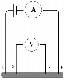
I want to use these strips to perform a four terminal sensing measurement on the conductivity of my printed ink strips. In most documentation I find that the distance between points 1-2 and 3-4 in the image below is smaller than the distance between points 2-3.

However the mask I created for depositing the aluminium on my substrates leaves four strips of aluminium with equal distances (see image below) 10 mm from center to center.
[PLAIN]http://image.bayimg.com/hapbaaach.jpg
the strips of aluminium left on the substrate will have a width of 1.5 mm.
The actual question is whether I can use R=U/I, simply ohms law, or whether I need to use a correction factor like discussed in Haldor (please refer to attachment), R=G * U/I.
The strips I will be printing across the aluminium strips will have a width of 100-1000\mum depending on my printing settings. the thickness of my print will be approx 10 times smaller.
I hope I cleared out my question, If you need anything else please let me know.
Thank you :)
Attachment: Haldor
http://dl.dropbox.com/u/1073056/Handige%20eBooks/Haldor%20weerstandsbepaling.pdf"
I want to use these strips to perform a four terminal sensing measurement on the conductivity of my printed ink strips. In most documentation I find that the distance between points 1-2 and 3-4 in the image below is smaller than the distance between points 2-3.
However the mask I created for depositing the aluminium on my substrates leaves four strips of aluminium with equal distances (see image below) 10 mm from center to center.
[PLAIN]http://image.bayimg.com/hapbaaach.jpg
the strips of aluminium left on the substrate will have a width of 1.5 mm.
The actual question is whether I can use R=U/I, simply ohms law, or whether I need to use a correction factor like discussed in Haldor (please refer to attachment), R=G * U/I.
The strips I will be printing across the aluminium strips will have a width of 100-1000\mum depending on my printing settings. the thickness of my print will be approx 10 times smaller.
I hope I cleared out my question, If you need anything else please let me know.
Thank you :)
Attachment: Haldor
http://dl.dropbox.com/u/1073056/Handige%20eBooks/Haldor%20weerstandsbepaling.pdf"
Last edited by a moderator: