How to understand power stage circuits with transistors (undergrad level)?

AI Thread Summary
Understanding power stage circuits with transistors involves recognizing the role of biasing resistors, which are crucial for providing a small quiescent base current to turn the transistors slightly "on" and prepare them for signal response. In a push-pull amplifier configuration, each transistor handles half of the sine wave, allowing for efficient power gain calculations. The power gain can be determined by the ratio of output to input power, which is derived from the resistances in the circuit, specifically noting that the output power is driven by an 8-ohm load while the input is influenced by a 1000-ohm resistor. There is some debate about the exact power gain value, with considerations for how current flows through the resistors during different signal phases. Overall, a clear understanding of bipolar transistor operation and circuit configuration is essential for grasping these concepts effectively.
Master1022
Messages
590
Reaction score
116
TL;DR Summary
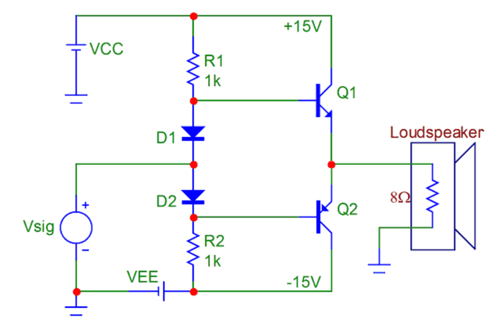
When I look at some circuits, I often get overwhelmed when there are transistors and diodes and I have no idea how to make much sense of it at a detailed level. For example, in this power stage B amplifier, what is the point of the resistors ## R_1 ## and ## R_2 ## in the circuit? Furthermore, how are they set if we have a power gain target in mind?
Hi,

When I look at some circuits, I often get overwhelmed when there are transistors and diodes and I have no idea how to make much sense of it at a detailed level. For example, in this power stage B amplifier, what is the point of the resistors ## R_1 ## and ## R_2 ## in the circuit? Furthermore, how are they set if we have a power gain target in mind?

Screen Shot 2021-04-23 at 11.43.07 AM.png


Questions:
1) What is the point of the biasing resistors?
I read that "R1 and R2 are necessary to bias the diodes and to provide a small quiescent base current bias for Q1 and Q2"
Might be a silly question, but what does that actually mean?

2) How do we use this circuit to find what the 'power gain' is?

Apologies if the question isn't clear. Perhaps I just need to find a clear explanation of this circuit online, but all these online tutorial websites don't seem to provide information in a useful way for me.

Many thanks in advance
 
Last edited by a moderator:
Engineering news on Phys.org
A bipolar transistor is naturally "off" unless we inject a small current into the base. So no current flows from emitter to collector until we do something. The purpose of the bias is to turn the transistor slightly "on" so it is ready to respond to a signal. With a push-pull amplifier like this, each transistor handles half of the sine wave, taking it in turns to fully conduct.
I notice that the two transistors are arranged in the Emitter Follower arrangement. In this case, very roughly the input and output voltages are the same. So Vsig appears across both the input and output. The power it is delivering is V^2/R. So at the input, Vsig is driving a 1000 Ohm resistor and the input power is V^2/1000. At the output, a voltage equal to Vsig is driving 8 Ohms. So the output power is V^2/8. The ratio of output to input power gives us the power gain, which is approx V^2/8 . 1000/V^2 = 1000/8 = 125.
Due to the push-pull action, each transistor works for half the time, but the result for power gain is the same as for a single ended amplifier.
 
  • Like
  • Informative
Likes Master1022 and DaveE
@Master1022 Well think about it, the schematic shows two bipolar transistors one being PNP and the other NPN. I suggest you first google about how bipolar transistors work and then this simple schematic will become more clear for you.

In short bipolar transistors work as current controlled switches. For a given applied current to the transistors base, a given larger current will flow from emitter to collector.

Now what you want in an amplifier is that your input signal controls your current and so controls your output but as you can probably see you cannot just connect your input signal positive to both transistor bases at the same time as that won't work so you need to connect the transistor bases in a circuit and then connect the input signal to that circuit. Remember that amplifier inputs are time varying waveforms so whenever the waveform is positive current flows in one direction while when the waveform reverses current flows in the other direction , this then makes the current to flow in the resistor biased diode connected circuit and eventually "drives" the bipolar transistors.
Think of it as a much smaller current controlling a much larger one.The resistors bias the transistor bases to a certain voltage , lower than the supply voltage, the values are high so that very small current flows through them.
The input signal path is then the one that controls the base current.
Note that this is a very simple schematic and real amplifier employ multiple stages of transistors and biasing because each stage can only amplify the input signal by a certain amount. For a single stage schematic you would need a very strong input signal to drive the output transistors directly. as for your second question @tech99 already beat me to it.
 
Thank you @tech99 and @artis for your replies. This definitely makes more sense now.

Just a quick follow up, should the power gain be 72.5 instead of 125? I was thinking this because there are two 1 kOhm resistors
 
@Master1022 at any given time the input signal is only passing current through one of the resistors not both.
For example when the input signal is positive (the positive half cycle of a sine wave test signal for example) current then goes to the negative rail of the amplifier through the resistor. When the input signal changes polarity to negative current goes to the other side.
Also as you can see there are diodes in series so for given polarity input signal current can only go one way as it would be blocked from going in the other direction.

At the output on the other hand the load is always 8ohm irrespective of which way the current flows.
 
Thread 'Weird near-field phenomenon I get in my EM simulation'
I recently made a basic simulation of wire antennas and I am not sure if the near field in my simulation is modeled correctly. One of the things that worry me is the fact that sometimes I see in my simulation "movements" in the near field that seems to be faster than the speed of wave propagation I defined (the speed of light in the simulation). Specifically I see "nodes" of low amplitude in the E field that are quickly "emitted" from the antenna and then slow down as they approach the far...
Hello dear reader, a brief introduction: Some 4 years ago someone started developing health related issues, apparently due to exposure to RF & ELF related frequencies and/or fields (Magnetic). This is currently becoming known as EHS. (Electromagnetic hypersensitivity is a claimed sensitivity to electromagnetic fields, to which adverse symptoms are attributed.) She experiences a deep burning sensation throughout her entire body, leaving her in pain and exhausted after a pulse has occurred...
Back
Top