Simple Common Emitter Amplifier

In summary, the transistor is not behaving as expected and the math seems correct, but there may be a problem with the β range.
  • #1
Helipil0t
2
0
Hey guys. I'm jumping into the world of electronics out of boredom and curiosity and am trying to wrap my mind around a few things. I'm on the topic of Transistors presently and have spend many hours learning about it's different modes of operation. I'm a bit confused about the Forward Active mode and was hoping someone could help me out. I think I understand the math as I will lay out. The problem is applying it to a real world example on my breadboard. For some reason the math doesn't add up to what I'm seeing. So here goes. Case in point:
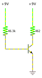
attachment.php?attachmentid=68513&stc=1&d=1397127209.png


A simple common emitter circuit consisting of the following measuring in at;
Power supply = 9.04V
Rb Resistor = 46.3kΩ
Rc Resistor = 462Ω
2N3904 Transistor with a β of 100 to 300 and Vbe = 0.628V

So first things first. Figuring out what mode the Transistor is operating at. For which it's my understanding that we solve the Forward Active model for DC and look at the resulting Vce to see where it lies;

Ib = Vcc - Vbe / Rb
= (9.04 - 0.628) / 46300
= 0.1816 mA

Ic = βIb
= 100(0.1816)
= 18.16mA

Vce = Vcc-(Ic)(Rc)
= 9.04 - (18.16mA)(462Ω)
= 0.65V > 0.2 ∴ Forward Active

With the Vce being greater than 0.2v (from Vce(sat) on the data sheet), The above should represent the circuit's behavior. So I slap this circuit together on my breadboard and start measuring using my multimeter.

I get a reading for Ib of 0.18mA which I expected. But then I measure Ic, I get 0.65mA.
Which doesn't seem right at all. I tested the BJT and swapped it out with a new one and I get the same reading. Tried using a different multimeter. (my Fluke 85 III was just calibrated last month) Same reading. Why am I only getting a gain of 3.6 when it should be at least 100?? I'm getting a voltage drop across Vce of 8.6V?? Am I doing something wrong. I laid the circuit out on a circuit simulator and it shows Ic at 18mA. So clearly the math is right. I get on the edge of understanding something and stuff like this happens. :confused: Can someone please help make me understand what I'm doing wrong and point me in the right direction.

Thanks!

Ps. My first post with this community. :biggrin: Cheers!
 

Attachments

  • CE_Circuit.png
    CE_Circuit.png
    1.2 KB · Views: 542
  • NPNDataSheet.pdf
    317.6 KB · Views: 255
Last edited:
Engineering news on Phys.org
  • #2
Check your transistor pinout. Make sure you are identifying the C B & E correctly. Some configurations are different and some manufacturers are different. Please measure the voltage across the 462 ohm resistor and post your results.

The setup you show is highly dependent on the Hfe (closely related to the Beta) of the individual transistor and as such, is really only useful in a mass production design as a switch. It does have other uses such as to frequency multiply, but advanced from your intentions at the moment.
 
  • #3
I was hoping it was that simple. :smile: I was convinced that I had the pinout correctly identified. Turns out another close look made me realize I was wrong. I did previously wonder if it was upside down and so I flipped it around once but was getting a 0 reading for Ic. I just assumed it was acting as a diode. After reading your reply I read the pinout diagram and tried again and realized my meter was set to μA, too high resolution to catch the current. Rookie mistake; one that I shouldn't of wasted your time with.

Here are the results:
Ic = 19.13mA
Ib = 0.1782mA
VRc = 8.82V
VRb = 8.27V
Vce = 0.22V
β = 107.35

The new math using β=107.35 predicted Ic = 19.50mA.. which is pretty close. I don't have an accurate measurement for the 47K resistor. I can only get 46.3K which would throw the numbers off a bit. I'll work the math backwards later to get Rb for fun.

I can see that having a β range of 100 to 300 would be problematic in this application. I was simply trying to get the concept straight in my head before I move on to darlington pairs. Out of curiosity though, what would be a good transistor that has a more predictable reliable β?

Finally I want to thank you for taking a second to respond. I appreciate it. Not sure how deep I'm going to go with this new found hobby. It looks like quite the rabbit hole. I'm interested enough to see where it takes me. Cheers! :approve:
 
  • #4
As for the β, there is no answer. This is a parameter that varies widely among each batch and manufacturer. Same holds true for any FET or MOSFET transistor, they all vary, and temp has an effect to cause variations as well.

The engineering education teaches one how to deal with the varying gain issue with various biasing techniques. The wiki linkBipolar transistor biasing provides a brief explanation on various configurations and how the change of the β (or Hfe) is minimized with each different technique.

As stated before, the configuration you present is perfect as a switching circuit, to turn on a light, power a relay, etc. You learn about each different configuration and put it in your toolbox for use when appropriate.

Have fun! This is a fun hobby and job for many.
Putting a little electronics knowledge with some of the low cost microcontrollers is even more fun with all the different things you can do!

Again have fun!
 
Last edited:
  • #5


Hello! It's great to see your interest and enthusiasm in learning about transistors and electronics. The common emitter amplifier circuit is a fundamental circuit in electronics and it's important to understand its operation.

First, let's make sure we are on the same page about the circuit. The common emitter amplifier consists of a transistor, a voltage source (Vcc), and two resistors (Rb and Rc). The base of the transistor is connected to the voltage source through Rb, and the collector is connected to the voltage source through Rc. The emitter is connected to ground.

Now, let's address your confusion about the forward active mode. The forward active mode is when the transistor is biased in a way that allows current to flow from the collector to the emitter. In this mode, the transistor acts as an amplifier, with the base current (Ib) controlling the collector current (Ic). In your circuit, you have correctly calculated that the transistor is operating in the forward active mode.

Next, let's look at your calculations. Your calculations for Ib and Ic are correct. However, your calculation for Vce is not. The correct equation for Vce is Vce = Vcc - (Ic*Rc) - Vbe. This takes into account the voltage drop across the base-emitter junction (Vbe), which you have not accounted for.

Now, let's address the issue with your measurements. It seems like your multimeter may not be reading accurately. It's possible that there could be a problem with the circuit or with the multimeter itself. I would recommend checking your circuit connections and trying with a different multimeter if possible.

Finally, it's important to remember that the transistor's beta (β) is not a fixed value, it can vary depending on temperature and other factors. So the gain (β) you calculated may not be the exact value you observe in the circuit.

I hope this helps clarify some of your confusion and gets you on the right track with your circuit. Keep experimenting and learning, and don't hesitate to ask for help when needed. Happy exploring!
 

1. What is a Simple Common Emitter Amplifier?

A Simple Common Emitter Amplifier is a type of electronic circuit used to amplify a small input signal to a larger output signal. It is commonly used in audio and radio frequency applications.

2. How does a Simple Common Emitter Amplifier work?

A Simple Common Emitter Amplifier works by using a transistor to amplify the input signal. The input signal is applied to the base of the transistor, and the amplified output signal is taken from the collector. The emitter is used as a common connection between the input and output circuits.

3. What are the components of a Simple Common Emitter Amplifier?

The main components of a Simple Common Emitter Amplifier include a transistor, resistors, and capacitors. The transistor acts as the amplifying element, while the resistors are used to bias the transistor and control the gain of the amplifier. Capacitors are used to block DC signals and allow only AC signals to pass through.

4. What is the gain of a Simple Common Emitter Amplifier?

The gain of a Simple Common Emitter Amplifier is the ratio of the output voltage to the input voltage. It is typically denoted by the symbol "β" and can range from a few tens to several hundred, depending on the circuit design and components used.

5. What are the advantages and disadvantages of a Simple Common Emitter Amplifier?

The advantages of a Simple Common Emitter Amplifier include its high voltage gain, low input impedance, and low output impedance. However, it also has some disadvantages, such as its sensitivity to temperature changes and its susceptibility to noise and distortion. Additionally, it requires careful biasing and can be affected by variations in transistor characteristics.

Similar threads

  • Electrical Engineering
Replies
3
Views
1K
  • Electrical Engineering
Replies
9
Views
5K
Replies
10
Views
1K
Replies
68
Views
4K
  • Electrical Engineering
Replies
17
Views
3K
Replies
2
Views
1K
  • Engineering and Comp Sci Homework Help
Replies
7
Views
896
  • Electrical Engineering
Replies
5
Views
2K
Replies
12
Views
2K
  • Electrical Engineering
Replies
1
Views
2K
Back
Top