Simple RC Hardware Circuit Understanding -- Questions

AI Thread Summary
The discussion revolves around understanding a specific RC hardware circuit, particularly the nature of signals at inputs Signal1 and Signal2, which are suspected to be from current transformers. There is confusion regarding whether these signals are AC or DC and how they interact with components like capacitors and resistors in the circuit. Participants emphasize the need for a complete schematic to accurately analyze the circuit's purpose and behavior, as the current fragment lacks clarity. Additionally, there are concerns about the values of capacitors and the implications of using incorrect components in the circuit design. The conversation highlights the importance of clear communication and complete information for effective circuit analysis and understanding.
PhysicsTest
Messages
246
Reaction score
26
TL;DR Summary
Need to understand the hardware circuit
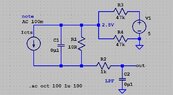
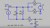
I need to understand the below hardware circuit
1650459214157.png


I am not sure about the type of the signals at signal1 and signal2, i have assumed DC signals initially. Then when i simulated in LT spice, the signal at Output is +5V. But if i assume the signals at signal1 and signal2 as Sine wave, then C1 and R1 will be like a filter circuit, am i correct? But what is the main purpose of the above circuit? Some information i decoded is signal1 and signal2 are coming from the connector, and they are Current transformer signals of the phase currents. Please help me to decode this.
 
Engineering news on Phys.org
If V1 and V2 are AC sources that can be different, it is not good to have them directly driving the capacitor C1 (which is an AC short). Is this just a practice circuit that you made up?
 
I am not sure if the signals Signal1 and signal2 are AC or DC, if AC signals are not correct, then they should be DC signals and if they are same,could you please tell me the purpose of the circuit if they are DC signals?
In the actual circuit V1 and V2 are not mentioned only for the simulation purpose i have added V1 and V2. The connection at output is going to the micro controller.
 
PhysicsTest said:
In the actual circuit V1 and V2 are not mentioned only for the simulation purpose i have added V1 and V2.
Can you please provide a link to the original source.
 
  • Like
Likes berkeman
It is a schematic given by friend to decode. I am only picking in parts to understand.
 
It would help if we could see the whole schematic and know what the intended purpose is. Looking only at some parts of a circuit may not may not be useful.
 
C1 and C2 have values of "0.1 Meg" farad ?
Are you sure those should not be something smaller, like maybe 0u1 farad ?
 
  • Wow
Likes berkeman
berkeman said:
It would help if we could see the whole schematic and know what the intended purpose is. Looking only at some parts of a circuit may not may not be useful.
I want to understand a circuit but no one is explaining that. I know it may have impact with remaining circuit, but I am not interested right now, just want to understand the behaviour of the circuit.
 
PhysicsTest said:
just want to understand the behaviour of the circuit.
Beyond the capacitor value errors, you have drawn the circuit with 3 inputs and no outputs. How are we supposed to guess what transfer function you want to discuss?
 
  • Like
Likes dlgoff
  • #10
The output is below R2 which goes to micro controller.
 
  • #11
PhysicsTest said:
In the actual circuit V1 and V2 are not mentioned only for the simulation purpose i have added V1 and V2.
If they are not inputs in the actual circuit, it is probably not a good idea to include them in the analysis. So your input is V3 and the output is the labeled node above C2? And what are the corrected values for the capacitors?
 
  • #12
I think my English is bad, Signal1 and Signal2 are inputs(if they are DC or AC I do not know), output (output in schematic) signal is going to micro. V3 is the 5V power supply.
 
  • #13
PhysicsTest said:
I think my English is bad, Signal1 and Signal2 are inputs(if they are DC or AC I do not know), output (output in schematic) signal is going to micro. V3 is the 5V power supply.
Well, the circuit still makes little sense to me. If V3=5V, that sets the bias voltage between R3 and R4 initially to 2.5V. But having V1 be a DC power supply then makes no sense, since that voltage is already set to 2.5V. But if V1 is an AC source, then it makes no sense to have V2 where it is, since it is an AC short via C1. So as drawn, I don't think V1 can be either AC or DC, and similarly V2 makes no sense where it is placed.

If there were no V2 source and V1 were an AC source, you could calculate (and simulate) the transfer function from V1 to the "Output" node. It looks at first glance to be a sort of a bandpass transfer function, with some modifications.

Again, it would be best to see the whole original circuit diagram, hopefullyl without the capacitor value errors shown on your LTSPICE rendition of the circuit.
 
  • #14
Aside from the many practical issues raised, which I'll leave to others, this is just an electrical network problem. You can express each component with it's complex impedance and find what you want with the normal circuit analysis tools (KVL, KCL, Thevenin-Norton source transformations, etc.). If you just view this as a math problem, it doesn't matter what the voltage sources actually are; ##v_1(t)## is a perfectly adequate variable name. If you have numbers to put in, like ##R3=4.7K##, then you'll do that as the last step.

Are you familiar with complex impedance values?

My personal preference would be to redraw that schematic with inputs on one side and outputs on the other side. That can make the analysis quick using some obvious shortcuts. What can you see about the node voltages? Do you actually care about every detail, like the current through R4, for example?

20220420_124950.jpg


PS: Sometimes simulators aren't worth the effort required. Don't go down that path (ever) without first thinking about the circuit in question. I claim there is no better way to understand a network like this that to at least try conventional network analysis first. Use the simulator when you have to, not before.
 
Last edited:
  • Like
Likes PhysicsTest
  • #15
DaveE said:
I claim there is no better way to understand a network like this that to at least try conventional network analysis first.
I claim:
The first step must be to identify what the circuit is required to do.
The second step will be to draw an accurate schematic.
The simulation step requires the first two steps be completed.

We have been given an incorrectly drawn schematic, for an unspecified task.
In this case, explaining how the circuit actually does it's job, is impossible.
 
  • Like
Likes berkeman
  • #16
Baluncore said:
We have been given an incorrectly drawn schematic, for an unspecified task.
In this case, explaining how the circuit actually does it's job, is impossible.
Agreed. And the OP refuses to post the full schematic as he received it, saying that he's only posting "the part that he wants to understand", after he has converted it incorrectly into an LTSPICE schematic to try do understand with simulation. I'm about to close this thread and issue a warning/infraction, unless the OP comes back with a very satisfying reply...
 
  • Like
Likes Tom.G and dlgoff
  • #17
Yes, the words of the OP make no sense at all.
 
  • Like
Likes dlgoff and berkeman
  • #18
Please find the circuit copied in the path . RA0, RA1, RA2 go to the micro controller. Is the circuit correct? If it is wrong i will stop analyzing.
 
  • #19
Where do the Current Transformers connect to that circuit? It's for a 3-phase AC Mains current measurement device?
 
  • #20
Yes.
 
  • #21
berkeman said:
Where do the Current Transformers connect to that circuit?
 
  • #22
I am not sure I only have this part of the circuit. Target is to write firmware to display current, but I am not able to understand the conversion formula. Will I be able to do with this part of schematic? What else I need to know?
 
  • #23
PhysicsTest said:
Is the circuit correct?
How would we know what you want? Sure, whatever, it can be correct if you like.
You'll get better answers if you ask clear complete questions.
 
  • #24
PhysicsTest said:
I am not sure I only have this part of the circuit. Target is to write firmware to display current, but I am not able to understand the conversion formula. Will I be able to do with this part of schematic? What else I need to know?
Okay, as you can tell we are very frustrated with the incomplete information you are providing, but since you are trying to learn, I'll try to make a couple of guesses and try to get you to the next steps. Lordy.

So, Current Transformers come in two types -- with and without "burden resistors". Those with burden resistors expect to be coupled into fairly high impedance measuring circuits, and use the burden resistors to convert the sensing current into an output voltage that you read with your microcontroller (uC).

Current Transformers without a burden resistor are meant to be used with your circuit that senses the output/secondary current of the CT, per the datasheet specs of the CT.

For CTs that have a burden resistor, they will specify what the conversion transfer function is, very typically you get 0.333Vrms output voltage for a 10Arms (or whatever current) input with a single wire turn through the CT core.

So the schematic you posted is ambiguous for CT measurements in several ways. First, the resistances and impedances of that circuit are medium, so too low to be used with CTs that have a burden resistor integrated, and strangely high for a raw CT. Whatever.

And since you are not able to explain how the three CTs are connected for the 3-phase current measurement, my best guess is that each CT has one side (non-dot side of the winding) grounded, and the other (dot) side connected to the schematic nets 4-5-6. This would give you an AC input voltage at AC Mains frequency on each of those "inputs" to the circuit, with a filtered version available at the three nets that you say are routed to your uC for digitizing.
 
Last edited:
  • Informative
  • Like
Likes PhysicsTest and dlgoff
  • #25
My take on the CT interface diagram in post #18 is as follows.

R1 with R22 divider produces DC bias = 2.5 volts, with R thevenin = 4k7 / 2 = 2k35

C1 = 0u1 farad; in parallel with; R19 = 10E = 10R = 10 ohm, (1/4 watt); is the burden for the CT. Shown as terminals 1 and 6.

R24 = 1k; in series with; C6 = 0u1; forms a low pass filter to the analog input port RA0.

Note that the Rth of 2k35 is in series with the 1k, so low pass has R = 3k35 with 0u1 F.

Software must discover the exact input voltage for zero current since 4k7 dividers are otherwise uncalibrated.
 
Last edited:
  • Like
Likes PhysicsTest
  • #26
Thank you very much for the clarifications, I am very poor in analyzing the circuits, hence based on the comment provided by DaveE i rearranged the circuit as below which was really helpful approach i have to follow,
1650634595990.png

Regarding the primary current calculations this is the formula i came across
##R = \frac{V_{CT}*N} {I_p}##
##I_p = \frac{V_{CT}*N} {R}##
So for example if i measure ##V_{CT} = 1.25V, N = 1000, R = 10##
##I_p = \frac{1.25 * 1000} {10} = 125Amps##
Are the above calculations correct?
I did not understand the statement
Software must discover the exact input voltage for zero current since 4k7 dividers are otherwise uncalibrated.
How do i do this?
 
  • #27
PhysicsTest said:
Are the above calculations correct?
We. are. not. mind. readers.

If you're asking if ##\frac{1.25 * 1000} {10} = 125##, then yes. That's what my calculator says too.

OTOH,
I don't know what ##R## is.
I don't know what ##V_{CT}## is.
I don't know what ##N## is.
I don't know what ##I_p## is.
I don't know what's connected to terminal ##1##.
I don't know what's connected to terminal ##6##.
I don't know what's connected to terminal ##RA0##.
I don't know what "##10E##" means when you write that next to a resistor.

I think I have a pretty good guess, but what's the point in my guessing in order to check your work.

PhysicsTest said:
I did not understand the statement
Me either. In fact, I don't even know what the statement was.

Try again. Better (complete) questions will get better answers.
 
  • #28
DaveE said:
We. are. not. mind. readers.

If you're asking if ##\frac{1.25 * 1000} {10} = 125##, then yes. That's what my calculator says too.

OTOH,
I don't know what ##R## is.
This is as per post #25, R is the burden resistor
C1 = 0u1 farad; in parallel with; R19 = 10E = 10R = 10 ohm, (1/4 watt); is the burden for the CT. Shown as terminals 1 and 6.
DaveE said:
I don't know what ##V_{CT}## is.
This is the Current Transformer voltage read by the micro controller. Here for example i am assuming the micro is reading a voltage of 1.25V.
DaveE said:
I don't know what ##N## is.
N is the number of turns assuming it to be 1000, for calculation
DaveE said:
I don't know what ##I_p## is.
This is the primary current flowing from the phase terminals. (R,Y,B), which is want i have to calculate and display on LCD.

DaveE said:
I don't know what's connected to terminal ##1##.
I don't know what's connected to terminal ##6##.
These are connected to the current transformer phase terminals.
DaveE said:
I don't know what's connected to terminal ##RA0##.
This will go to the micro controller ADC input pin.
DaveE said:
I don't know what "##10E##" means when you write that next to a resistor.
This is 10 Ohm resistor.
 
  • #29
PhysicsTest said:
Software must discover the exact input voltage for zero current since 4k7 dividers are otherwise uncalibrated.
How do i do this?
The voltage to the analog input when no current is flowing in the CT will be close to 2.5 V. The resistors in the voltage divider may be slightly different, so you need to find just what voltage represents zero current. Without the CTs being connected, read each analog input to identify zero for each channel.

Note that a CT will often have an internal resistor of maybe 470R, that is to protect the insulation from overvoltage arcs if you unplug it from the burden on the PCB. That unknown protection device may change the calibration scale slightly.

Avoid decimal points. "0.1μ" is better written in LTspice as "0u1". It may then be displayed as "0μ1" if that option is turned on.
Avoid the exponential "10E", use instead the more common "10R".
"10E" is actually a suppressed zero exponent, floating point "10E0" = "1E1" = 10.

Never put units on component values, or on voltage and current sources.
1F is not one farad, it is one femtofarad. 1A is not one amp, it is 1e-18 amp.
 

Attachments

  • Schematic.jpg
    Schematic.jpg
    43.5 KB · Views: 158
  • TransferFunction.jpg
    TransferFunction.jpg
    41.4 KB · Views: 134
  • TransRespGain.jpg
    TransRespGain.jpg
    49.5 KB · Views: 130
  • TransducerGain.jpg
    TransducerGain.jpg
    47.5 KB · Views: 143
Last edited:
  • Like
Likes PhysicsTest
  • #30
I am trying to solve the schematic manually using node equations
1650710808493.png

The current through C1 is i1, R1 it is i2, through R4 is i1+i2+icts.
##V_{C1} = V_{R2}##
##\frac{\int{i_1} dt} {C_1} = i_2 R1## -> eq1.1
##2.5 - i_2R_1 - (i1+i2+i_{cts})R4 = V_{out}## -> eq1.2
##i_{cts} + i_1 + i_2=0 ## -> eq 1.3

Are the equations correct to solve for ## V_{out} ##.
 

Attachments

  • 1650709312553.png
    1650709312553.png
    31.8 KB · Views: 128
  • #31
OK, I didn't want to keep beating this horse but I guess I'll have to say it again. Define your terms. Be consistent.

I don't know what ##V_{R2}## is, so I don't know why you said ##V_{C1}=V_{R2}##. In fact I don't even know what ##R2## is because you posted two schematics with different names for the resistors.

It would be conventional for ##V_{R2}## to be the voltage across ##R2## with a polarity clearly defined in a schematic (which isn't there, yet). That would be either with a current direction clearly defined or the voltage polarity indicated. Look into "passive sign convention" for more about that. So, for example, you did a good job of telling us that ##i_2## flows through ##R1##, but you didn't tell us the direction, so I can't say if your eq 1.1 is correct or not.

Same comments for ##V_{C1}## , ##i_1## , everything, really.

In this case I can't even really guess what you actually meant, because I don't think ##V_{C1}## is equal to any other branch voltage. So there might be a problem there. However, there are also problems with your other equations, but I don't think it's really worth commenting on those until we have a bit more structure in your approach, and communication.

The thing about circuit analysis (using KVL, KCL, etc.) is that the solution is relatively easy, even sort of automatic when you go through all of the steps. The hard part, the part the messes everyone up, is that they don't define all of the voltages and currents well. They try to skip steps, which is often quite tempting. This an analysis technique where how you set up and define the problem is by far the most important part. Khan Academy has some really good tutorials about circuit analysis. I would suggest watching some of those next.

If you want a STEM career, like in physics or EE, you need to learn to define and communicate the details clearly. Slow down, be more careful.
 
Last edited:
  • Like
Likes Klystron, berkeman, PhysicsTest and 1 other person
  • #32
It also helps if currents have a direction marked with an arrow.
 
  • #33
Thank you for all the help, i know i am confusing all, circuit analysis is always tough for me. I am doing another attempt
1650775616853.png


Loop1 : Consisting of elements C1 and R1
## \frac{-\int I_1dt} {C1} + I_2R1=0 ## -> eq1
Loop2: consisting of 2.5V, R1 and R4
##2.5 - I_2R_1-(I_1+I_2+I_{cts})R_4 = V_{out}## -> eq2
##I_{cts} = I_0\sin(\omega t)##
I need one more equation, Please help me if the equations are correct and where do i apply the next equation?
 
Last edited:
  • #34
Sorry, too busy to write a real reply. But that node labeled 2.5V is only 2.5V if there's no current being drawn through those 47K resistors. You can't leave R2 & R3 out, also C2 needs to be included. Those parts are in loops you haven't included yet.

But, good work on defining things, now we can all speak the same language.
 
  • Like
Likes PhysicsTest
  • #35
DaveE said:
But that node labeled 2.5V is only 2.5V if there's no current being drawn through those 47K resistors. You can't leave R2 & R3 out,
But it will always be 2.5V since the resistors are equal and by voltage divider rule, it shall be 2.5V.

DaveE said:
also C2 needs to be included. Those parts are in loops you haven't included yet
Loop1 : Consisting of elements C1 and R1
## \frac{-\int I_1dt} {C1} + I_2R1=0 ## -> eq1
Loop2: consisting of 2.5V, R1 and R4
##2.5 - I_2R_1-(I_1+I_2+I_{cts})R_4 - \frac{\int (I1+I2+I_{cts})dt} {C_2} = 0 ## -> eq2
##I_{cts} = I_0\sin(\omega t)## ->eq3

The current through ##R_2 = \frac{2.5} {4.7k} = 0.53mA ## ->eq4
Similarly current through ## R_3 = \frac{2.5}{4.7k} = 0.53mA ## ->eq5
## I_1 + I_2 = 1.06mA ## ->eq6
Can i use the above equations to solve for Vout?
 
  • #36
PhysicsTest said:
But it will always be 2.5V since the resistors are equal and by voltage divider rule, it shall be 2.5V.
The Thevenin resistance, Rth, of the 2.5 volt reference is 4k7 / 2 = 2k35 . That Rth is in series with the 1k0 of the LPF, making 3k35 total. If you ignore Rth, the transfer function will be incorrect.

You must close the circuit from ground of the LPF, to the ground of the bias network.

I still do not know what you are doing, nor why.
 
  • Like
Likes PhysicsTest
  • #37
Baluncore said:
I still do not know what you are doing, nor why.
The main reason why i am trying to do is, to derive an expression for Icts as a function of resistors and Vout. Develop firmware to use this formula calculate and display the Icts (additionally convert this into phase current) on lcd. Is my approach correct?
 
  • #38
Hi @PhysicsTest...
Now that you have defined the components and have an easy-to-read schematic, etc, let's try breaking the circuit down to the DC component and then add in the AC component.

We will be making a few assumption along the way, and later add in corrections to cover the assumptions.

For the first part let's try to find the DC voltage at the A/D converter input. We can ignore the CT and the capacitors for this, just assume they do not exist or are open circuits.

What IS needed is the input impedance of the A/D converter. We may decide later that this can be ignored if it is much higher that the circuit resistance values, but we don't know that yet!

Next would be to draw a schematic with the Voltage Source, the Resistors, and the Input Impedance of the A/D converter. From that you can calculate the 'Zero' reading at A/D input.

Now you get to make a decision. Is the calculated DC voltage at the A/D input enough different from the 2.5V 'Ideal' voltage to really matter? If you want to end up with the Complete design equations, this step is complete and you can ignore the next paragraph

For instance, if the voltage difference between using the A/D input, and assuming it is an open circuit is less than the A/D resolution, then consider the A/D as an open circuit and use the 2.5V divider voltage. (In the real world, there may be a variable resistor in the R2 - R3 divider network to trim the Zero voltage.)

Now consider the situation with the CT connected. The CT will have some internal resistance which is in parallel with the 10 Ohm resistor. The equivalent parallel resistance can be substituted in the equation derived above for the 'Zero' DC input to the A/D converter...
Or, again, you may want to substitute the equation for the parallel resistances into the DC equation derived above.

That completes the basic DC bias point calculation. If this was a design for producing many of these circuits, things like the resistors tolerances and maybe their resistance variation with temperature would also be accounted for.

Sorry for hijacking this thread, after you get the DC bias point completed, I will bow out and let the others here carry on their fine support.

Cheers,
Tom

p.s. Remember details count, and the more of them you supply the easier it is for everyone. (except maybe you when you have to type so much :wink:)
 
Back
Top