Can LCL Filter Convert AC to DC for Half Bridge Section?

Join the discussion
Ask a follow-up here, or get your own question answered by working scientists, mathematicians and engineers — people, not an autocomplete.
Real named experts · corrections over time · the nuance an AI answer skips
39 replies · 5K views
PhysicsTest
Messages
260
Reaction score
27
TL;DR
Understanding the output of the LCL filter.
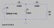
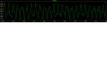
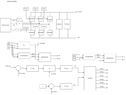
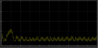
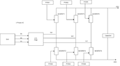
I am trying to simulate the active converter, I have seen in you tube video the output of the grid 3 phase voltage is given to LCL filter, the output of the LCL filter is then given to the half bridge section. I assume that the output of the LCL filter is a DC instead of the sine wave, as it is given to the half bridge section, is my understanding correct? Or sine wave can also be given to half bridge? VDC will be the output i hope, that is what i am trying to achieve DC from AC. Please advise. I also tried to simulate a simple LCL circuit in Ltspice, the output as shown when a sine wave of 50Hz given. I am bit confused with Inverter and converter, where is the difference happening, both use H bridge?
 

Attachments
  • Converter.png
    Converter.png
    6.4 KB · Views: 201
  • Circuit.png
    Circuit.png
    4.5 KB · Views: 198
  • Ouptut.png
    Ouptut.png
    8.1 KB · Views: 210
Last edited:
Engineering news on Phys.org
The 'T' filter is designed to prevent switching noise generated by the H-bridge from reaching the grid, and so causing EM interference.

I am surprised that the values for the L and C components are so large. It seems to be tuned to pass energy at 23 Hz. How did you select those values?

Can you please give a link to the video?
 
Sorry the LT spice model is created by me to understand the circuit, to verify the output of the filter, i have chosen random values of inductor and capacitor, the video is
 
From the video, the values of L1 and L2 are 500 uH, C1 is 100 uF.
This shows AC analysis of the symmetrical T filter. It is designed to allow 50 Hz to pass, but to stop HF noise from reaching the 3PH supply.
The way the AC to DC converter is drawn is very confusing.
It takes 415 V, 50 Hz, 3PH AC and switches it into the DC storage capacitor.

T-Filter.png

AC_analysis.png
 
  • Like
Likes   Reactions: PhysicsTest
What is the basic principle of converting AC to DC using Mosfet switches?
 
The controller measures the voltage on the 3PH lines. It measures the voltage on the capacitor. When the capacitor voltage falls, the controller momentarily connects two selected lines to the capacitor to increase the voltage. The way the converter is programmed will decide the behaviour. Maybe it is programmed to maintain a high power factor and a stable output voltage.
 
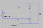
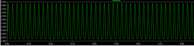
I am trying to learn the algorithm of Active converter, which i have to execute in Matlab, as a first step i saw a circuit and drawn in Ltspice, the output will be DC voltage with ripples, in the book the circuit is controlled using thyristor, i have redrawn using diodes. My initial confusion is, giving the negative portion of the sine wave to the bridge which is different from the ground. When i plot the output of the sine wave i get the below result, with the negative portion swing is reduced. But how do i understand the sine wave and ground different?
 

Attachments

  • rectifier.png
    rectifier.png
    2.4 KB · Views: 203
  • result_rectifier.png
    result_rectifier.png
    9.5 KB · Views: 169
PhysicsTest said:
But how do i understand the sine wave and ground different?
Reduce the load resistance from 1k to 100R. Then you will see the flat base.

Two diodes in the bridge must turn on before conduction occurs. That explains the missing 1.5 volts. Each is dropping Vpn=0.75 volt. Increase the voltage to 50 Vpk, and the 2*Vpn will be a minor problem.

Note that LTspice specifies the peak voltage of the sine wave, not the RMS.
 
Baluncore said:
Reduce the load resistance from 1k to 100R. Then you will see the flat base.

Two diodes in the bridge must turn on before conduction occurs. That explains the missing 1.5 volts. Each is dropping Vpn=0.75 volt. Increase the voltage to 50 Vpk, and the 2*Vpn will be a minor problem.

Note that LTspice specifies the peak voltage of the sine wave, not the RMS.
Surely i will try this, but before that i found another simple circuit compared to the above, with all the AC phases grounded, I want to understand which bottom diodes will be ON, it is very confusing.
1655640082626.png


I also simulated in the LTspice, my explanation is something like this when Va is Positive and greater than Vb and Vc, D1 is ON, D4 is OFF. Could you please explain me which of the bottom diodes will be ON in simple terms.
1655640282741.png
1655640184310.png
 
PhysicsTest said:
Could you please explain me which of the bottom diodes will be ON in simple terms.
The highest diode that will be conducting will be that on the most positive phase.
The lowest diode that will be conducting will be that on the most negative phase.
 
Let's just assume that D1 and D6 are conducting at time ##t_{16}##. That will create a voltage at the output of ##v_a(t_{16}) - v_b(t_{16})## let's call this ##v_{ab}##; this is pretending that the diodes don't drop any voltage when they're on, a convenient, but wrong assumption. For this to be correct, we must have ##v_{ab}## be greater than all of the other combinations (##v_{bc}, v_{ca}, v_{ba}, v_{cb}, v_{ac}##). Otherwise a different diode pair would conduct.

So, it's not the most positive or negative phase (wrt neutral) that determines the switching, it's the greatest phase difference. For example: when is the maximum value of ##sin(\omega t) - sin(\omega t +\frac{2\pi}{3})##? It turns out this isn't at ##\omega t=\frac{\pi}{2}## when ##sin(\omega t)## is maximum, it happens at ##\omega t=\frac{2\pi}{3}## (I think, you should probably check my math).

PS: Of course the switching doesn't happen at the maximum. For that you need to look for when the line to line voltages are equal, like ##v_{ab} = v_{bc}## etc.
 
Going through several websites and documents arrived at the following flow for the active converter. I have used the SVPWM technique to control the VDC voltage. Request to please provide review comments to update, updated the simulation in Matlab but some compile errors in svpwm block, i will rectify then i can share the results.
 

Attachments

  • FinalRectifier.png
    FinalRectifier.png
    12 KB · Views: 186
I do not understand how you can use MOSFETs in that topology to regulate the output voltage. The source must be connected to an extreme voltage that the drain never crosses, or the substrate diode will conduct.
 
I do not understand much but I have seen IGBTs being used, that is what is meant to use in place of MOSFETs?
 
An IGBT is a BJT with a control MOSFET connected between the base and collector. The IGBT has the same reverse conduction problem as the MOSFET.
 
We could use the diode in reverse direction?
 
PhysicsTest said:
We could use the diode in reverse direction?
You need to produce a circuit diagram that shows the actual components between the 3PH and the DC output. Then I will know which diode you are referring to, and how it is connected relative to the 3PH and DC.

It is possible that the MOSFET substrate diodes are being used with the second inductor of the T-filter for soft commutation of the converter.
 
  • Like
Likes   Reactions: DaveE
Thank you for support. I need to update the diagram including the diodes, I will update and share it, any comments on the other blocks.
 
Baluncore said:
It is possible that the MOSFET substrate diodes are being used with the second inductor of the T-filter for soft commutation of the converter.
Yes, I would expect they will commutate OK provided the controller doesn't do something wrong.
 
After simulation the results looks like this, the DC voltage does not regulate it goes to 0 and the set DC voltage is 800V. Any suggestions where the mistake could be?
 

Attachments

  • Output.png
    Output.png
    9.2 KB · Views: 172
PhysicsTest said:
Any suggestions where the mistake could be?
It is probably in the lack of documentation.
We have no idea what code you are running, or what happens in those rectangular blocks.
If you produced a complete circuit diagram of one of the MOSFET switches, that might explain everything.
 
If you could please install MATLAB trial version available, i can share the simulink model to open it. The rectangular boxes are directly the library components of the MATLAB simulink.
 
PhysicsTest said:
If you could please install MATLAB trial version available, i can share the simulink model to open it.
No. I do not have the space, nor the time to learn to use something I have no use for.
 
  • Like
Likes   Reactions: DaveE
Ok, few clarifications i want to calculate the max half wave / full wave rectifier DC output voltage from the input sine wave
1656393166249.png


If the input sine wave is
i=##A\sin(\omega t)##;
Dc_output = ##\int^{\frac{\pi}{\omega}}_{0} A\sin(\omega t)##
=##\frac{A}{\omega}[-\cos(\omega t)]^{\frac{\pi}{\omega}}_{0}##
=##\frac{2\sqrt2A_{RMS}} {\omega}##
But when see the answer it does not depend on the frequency, the answer is ##\frac{2\sqrt2A_{RMS}}{\pi}##.
Please help me to find how ##\pi## is arrived.
 
PhysicsTest said:
Please help me to find how π is arrived.
Wait, what? Is that really your question. It happens ALL THE TIME in sinusoidal stuff.
 
Sorry, anyway...
The DC value of a waveform means the average value. The waveform is repetitive, so as long as you average over complete cycles, the frequency doesn't matter. The average of the first cycle is the same as the average of the second cycle, which is the same as the average of the first and second cycles.

Like this:
What is the average value of the numbers 4, 8, 2, and 6?
What is the average value of the numbers 4, 8, 2, 6, 4, 8, 2, and 6?
What is the average value of the numbers 4, 8, 2, 6, 4, 8, 2, 6, 4, 8, 2, and 6?
What is the average value of the numbers 4, 8, 2, 6, 4, 8, 2, 6, 4, 8, 2, 6, 4, 8, 2, and 6?

Does the average value depend on how many cycles I ask about?
 
Last edited:
  • Like
Likes   Reactions: PhysicsTest
Ok thank you now i understand the answer shall be divided by the width of 1 cycle, ##\frac{\pi} {\omega}##.
Hence the answer will be ##\frac{2\sqrt2 A_{RMS}} {\pi}##. Thank you very much.
 
  • Like
Likes   Reactions: DaveE
For a sinewave, the average voltage is not the integral, but the Root Mean Square.
For; v = A * Sin(...), the average voltage will be; Vrms = A / √2 .

To build a prototype, you will need a circuit diagram. I see no point in simulating something that cannot be built. Can Simulink dump a circuit diagram, or a net list?
 
Baluncore said:
For a sinewave, the average voltage is not the integral, but the Root Mean Square.
For; v = A * Sin(...), the average voltage will be; Vrms = A / √2 .
Sorry, I know it's semantics, but..
The average value of a sine wave is zero. The RMS value is the RMS value, not the average. The world will be a better place if we can all stick with ##Avg(f(t)) = \frac{1}{T} \int_0^T f(t) \,dt## . It's a pretty good definition that has served us all well.