Discussing Stagger tuning in VHF receivers....

  • Thread starter Thread starter brainbaby
  • Start date Start date
  • Tags Tags
    Tuning
AI Thread Summary
The discussion centers on the concept of stagger tuning in VHF receivers, highlighting confusion over the effects on voltage amplification. It is noted that stagger tuning can reduce the total voltage amplification to half the value of the unstaggered configuration, while also allowing for equivalent voltage amplification per stage when bandwidth is decreased. Participants express uncertainty about the significance of the "one-half" factor, suggesting it may serve as a normalizing value rather than a strict mathematical rule. The conversation also touches on the importance of using amplifiers to buffer stages in stagger tuning, which allows for better control of impedance and avoids loading effects. Overall, the complexities of stagger tuning and its implications for circuit design remain a focal point of inquiry.
brainbaby
Messages
232
Reaction score
5
Hi Friends and Happy new year to all,

It confused me as I see two different statement yet explaining same thing…..

First para *in highlight states that stagger tuning of two single tuned circuits stagger to the amount equal to their bandwidth reduce the total voltage amplification of the resultant curve to HALF amount to the value obtained before stagger tuning.

and something different has been stated a little bit ahead..

Second para *in highlight states that after decreasing bandwidth to an amount and staggering the circuits to the new value of bandwidth obtained, the stagger pair voltage amplification will be the SAME as of the single tuned stage.

Why this discrepancy…??
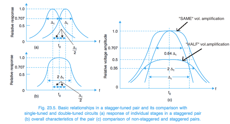
fig_stag.png


Thanks!
 

Attachments

  • 1_STAG.png
    1_STAG.png
    69.8 KB · Views: 732
  • 2 STAG.png
    2 STAG.png
    66.2 KB · Views: 650
  • fig_stag.png
    fig_stag.png
    30.4 KB · Views: 984
Engineering news on Phys.org
brainbaby said:
Second para *in highlight states that after decreasing bandwidth to an amount and staggering the circuits to the new value of bandwidth obtained, the stagger pair voltage amplification will be the SAME as of the single tuned stage.
Decreasing bandwidth (by raising Q, as he said) raises gain.
brainbaby said:
Why this discrepancy…??
I think he explained it.
upload_2018-1-2_1-39-19.png
 

Attachments

  • upload_2018-1-2_1-39-19.png
    upload_2018-1-2_1-39-19.png
    13.1 KB · Views: 617
Increase Q to increase gain according to relation Q = ƒr /BW is quite acceptable to me.

Screen Shot 2018-01-02 at 6.17.51 pm.png


where does one-half comes from. Is it the magic of staggered tuning.
or it could be thought like this..
In first para at a certain value of gain the circuits are staggered to a fixed similar amount delta 1.
now in second para...
At staggering tuning makes gain goes down to half of the two stages. But if any how the staggered amount is maintained constant and the gain is increased then still the stagger tuning will force the gain to reduce down to half but mathematically half of the product of increased gain will provide a value that will be equal to initial value of gain of single tuned circuit . So I think so that it is just a kind of compensation of an increased gain value.

But I am still doubt full about the existence of "one-half"...please clarify??
 

Attachments

  • Screen Shot 2018-01-02 at 6.17.51 pm.png
    Screen Shot 2018-01-02 at 6.17.51 pm.png
    15.9 KB · Views: 621
brainbaby said:
But I am still doubt full about the existence of "one-half".
Is it not just a normalising factor?
 
sophiecentaur said:
Is it not just a normalising factor?
The overall gain of two cascaded amplifier is equal to the product of their individual gain...but here in case of stagger tuning its half of the product of their indivdual gain...thats why I maybe thought like that...
Still isn't clear of "one half"
 
brainbaby said:
Still isn't clear of "one half"
If you read the link carefully it says the gain is half of the tuned version. The product of the gains at any particular frequency gives the overall gain (as you say) but the two gains are never A at the same frequency. With the appropriate stagger, you have a resulting net gain of half the unstaggered value. This '1/2' value only applies for one particular value of stagger. If you stagger them by a lot, the gain will be zero!
I think the link could have explained it better. :smile:
Aoverall (f) = A1(f) . A2(f)
but you know this already. The link has just picked a particular offset and made it appear that the result is for the general case.
 
  • Like
Likes brainbaby
Ya ...1/2 is not with the formula..which I initially thought it was...rather it is just to signify half value of the gain at a particular instant...an interim value

But still I am struggling with some doubt...
The amount of stagger tuning is same in both the paras. In first para it is delta 1 and in the second para it is some new value as the individual bandwidth is decreased...but technically both cases are same since the stagger amount is same and the individual gain increases by increasing the quality factor...now if gain is increased the product of the two will obviously be a larger value resulting in larger overall gain but stagger tuning is making it possible to have equivalent voltage amplification per stage as of single tuned stage...i.e after decreasing the bandwidth gain is increased by a factor of 1.4...i.e 1.4X1.4 = 1.96 nearly 2...but stagger tuning has done some background work or kind of compensation to make the gain equal to that of single tuned stage...I need that visualization...??
 
brainbaby said:
Ya ...1/2 is not with the formula..which I initially thought it was...rather it is just to signify half value of the gain at a particular instant...an interim value

But still I am struggling with some doubt...
The amount of stagger tuning is same in both the paras. In first para it is delta 1 and in the second para it is some new value as the individual bandwidth is decreased...but technically both cases are same since the stagger amount is same and the individual gain increases by increasing the quality factor...now if gain is increased the product of the two will obviously be a larger value resulting in larger overall gain but stagger tuning is making it possible to have equivalent voltage amplification per stage as of single tuned stage...i.e after decreasing the bandwidth gain is increased by a factor of 1.4...i.e 1.4X1.4 = 1.96 nearly 2...but stagger tuning has done some background work or kind of compensation to make the gain equal to that of single tuned stage...I need that visualization...??
Why not just go along with the Maths and forget any possible confusion about 'numbers' in that presentation? Calculate the passband shape for a range of offsets, leaving out any normalising factor. Graph plotting of a function is not hard and there are many apps that will do it for you. Most spreadsheets will let you do it and give you the "visualisation" that you want. Good practice at simple coding, too!
 
  • Like
Likes brainbaby
An amplifier does not have one gain, it has a transfer function that describes amplitude and phase relative to the input over a range of frequency. The product of two transfer functions is done at each frequency. If you measure the gain of two tuned circuits or amplifiers at different frequencies, then the product of those gains will be meaningless.

Stagger tuning overlaps the circuit responses in such a way that the transfer functions between the peaks cancel to give a maximally flat passband, while outside the band the transfer functions reinforce to steepen the skirts for greater attenuation.
 
  • Like
Likes NTL2009, brainbaby and sophiecentaur
  • #10
sophiecentaur said:
Most spreadsheets will let you do it

@Baluncore
Can you just provide me a spice simulation of a particular stagger tuned circuit at different value of staggering...
 
  • #11
I am trying to simulate this circuit but I am confused regarding selecting the component values and how should I select the centre frequency for the tuned circuit and how to stagger them to three different values so that I could compare the result for analysis.
What feature does spice provides for staggering two tuned circuits..

template.PNG
 

Attachments

  • template.PNG
    template.PNG
    1.9 KB · Views: 1,038
  • #12
Post your LTspiceFile.asc as LTspiceFile.asc.txt
There must be L, C and R in a tuned circuit to get a finite Q.
 
  • #13
please find the file below
 

Attachments

  • #14
brainbaby said:
I am trying to simulate this circuit but I am confused regarding selecting the component values and how should I select the centre frequency for the tuned circuit and how to stagger them to three different values so that I could compare the result for analysis.
What feature does spice provides for staggering two tuned circuits..

View attachment 218074
For stagger tuning the two resonant circuits are separated by an amplifier. As baluncore says, the resistances in each circuit must be specified and you must include the source resistance. Are you showing a constant voltage source? This would have zero resistance and would prevent the circuit from operating.
 
  • #15
tech99 said:
Are you showing a constant voltage source?
My voltage source is a sine wave ac source with AC amplitude of 100 and a dc offset of 1.
 
  • #16
brainbaby said:
My voltage source is a sine wave ac source with AC amplitude of 100 and a dc offset of 1.
You need to know the resistance of the source and ensure that the tuned circuit has the required total value of resistance across it. You also need to use the correct value of resistance across the secondary, and you need to consider the resistance/impedance of the measuring device. You need to separate the two stages using an amplifier. Your voltage of 100 sounds remarkably high and will overload most amplifiers.
 
  • #17
tech99 said:
Your voltage of 100 sounds remarkably high
mV surely?
tech99 said:
For stagger tuning the two resonant circuits are separated by an amplifier.
Not in the old days. The two resonant circuits would be linked by mutual Inductance (and some C, too). Buffering with an amplifier is a 'new' idea - I don't know just how new. The calculations for linked resonant circuits were much more complicated and, personally, I would have used tables (simulations were well in the future).
 
  • Like
Likes dlgoff and brainbaby
  • #18
sophiecentaur said:
mV surely?

Not in the old days. The two resonant circuits would be linked by mutual Inductance (and some C, too). Buffering with an amplifier is a 'new' idea - I don't know just how new. The calculations for linked resonant circuits were much more complicated and, personally, I would have used tables (simulations were well in the future).
There are (were) two methods of making a broadband RF amplifier, such as for TV IF.
The first is to use interstage coupling by two tuned circuits which are coupled together and provide a flat topped band pass response. This was usually called bandpass coupling
The second is to use single tuned circuits between stages, and to de-tune each of them in order to broaden and flatten the response. The latter is what I understand by Stagger Tuning. It avoids the need for accurate mutual coupling, and the performance of the two systems was fairly similar, I believe.
As you mention, there are normalised tables for finding the responses.
With the bandpass system, it is usual to tune each circuit in isolation to the same frequency. However, Terman discusses the effect of staggering for this case also, and I recall that the overall effect is similar to altering the mutual coupling.

.
 
  • Like
Likes sophiecentaur
  • #19
@brainbaby
Remove the .txt suffix to try this LTspice code. It does a sweep of peak separation to show product of stagger tuning.
 

Attachments

  • #20
Model has a perfect voltage follower Bvf, and duplicates the low frequency side to plot transfer functions of the frequency staggered circuits and the product of the staggered pair.
model3.png


dB voltage
dB3.png


Linear voltage
lin3.png
 

Attachments

Last edited:
  • #21
tech99 said:
The second is to use single tuned circuits between stages, and to de-tune each of them in order to broaden and flatten the response. The latter is what I understand by Stagger Tuning. It avoids the need for accurate mutual coupling, and the performance of the two systems was fairly similar, I believe.

@Baluncore ..What I don't understand here is what is the requirement of buffering the two stages by using a voltage follower...as I was expecting a mutual coupling between two tuned stages in order to analyse stagger tuning..
 
  • #22
You need to make two symmetrical tuned circuits with very similar Qs. That requires you control the input and output impedance of each circuit since the Q is determined by the R of RLC. The voltage follower isolates the circuits so the input resistance of the second does not load the output of the first.

You need also to be able see the combined response by offsetting the centre frequencies of the two resonators in a controlled manner. But once you couple two resonators you cannot see the individual response of either. The mutual coupling must also be changed to compensate for the difference in frequency.

A double tuned transformer must have very low coupling to prevent the two circuits merging into one parallel combination, with the inductors becoming one and the capacitors in parallel. But low coupling represents a loss of signal energy. The coupling can be made arbitrarily small without loss of signal by inserting an amplifier stage between the resonators. That was done with IF strips, where each stage had maximum gain at staggered centre frequencies. The tuned IF transformers also provided the imprdance matching and level translation of collector voltage to base voltage between gain stages. It used to take some time with a sweep generator to adjust all the inductors in an IF strip to give an acceptable response.

The dB plot shows clearly why the staggered resonators, each with a maximum gain of 0 dB can result in a wider, maximally flat passband with an attenuation of 6dB.
 
  • #23
Baluncore said:
offsetting the centre frequencies of the two resonators in a controlled manner.
I guess that controlled manner here signifies that the total offset amount of central frequency should be equal to the bandwidth of individual stage.??
 
  • #24
brainbaby said:
I guess that controlled manner here signifies that the total offset amount of central frequency should be equal to the bandwidth of individual stage.??
That is true for the simple situation if you want a maximally flat response. Maybe it is better to have some ripple and a steeper wall.

Here is a version without the buffer, cut for 5% coupling. See what happens when you change the coupling. Higher coupling locks the resonators and pulls the frequencies out, while lower coupling increases the losses. It demonstrates the advantage of amplifiers.
PF_far_couple_1.png
 

Attachments

Last edited:
  • #25
Baluncore said:
mutual coupling must also be changed to compensate for the difference in frequency.

What kind of compensation are you talking about..I mean what's the requirement, since both the method either mutual coupling or offsetting centre frequency flattens the response?
 
Last edited:
  • #26
brainbaby said:
What kind of compensation are you talking about..I mean what's the requirement, since both the method either mutual coupling or offsetting centre frequency flattens the response?
Both models change the centre frequency of the resonators in exactly the same way.

One method isolates the resonators with a stage amplifier giving two independent sets of three parameters to adjust, in time proportional to the third power.

The other method adds the difficult to adjust transformer coupling parameter, makes all seven terms interdependent and restricts the possible solutions. You must adjust 7 terms to set the BW centre frequency, flatness, Q=skirt symmetry and match input and output impedance, (they will be different). The time to do that will be uneconomic, proportional to the seventh power.

I cheated making the model by having equal input and output impedances, by not matching the Q and by tracking four tuning changes with the earlier version component values and the ratiometric sweep parameter, p.
 
  • #27
Baluncore said:
Both models change the centre frequency of the resonators in exactly the same way.

One method isolates the resonators with a stage amplifier giving two independent sets of three parameters to adjust, in time proportional to the third power.

The other method adds the difficult to adjust transformer coupling parameter, makes all seven terms interdependent and restricts the possible solutions. You must adjust 7 terms to set the BW centre frequency, flatness, Q=skirt symmetry and match input and output impedance, (they will be different). The time to do that will be uneconomic, proportional to the seventh power.

I cheated making the model by having equal input and output impedances, by not matching the Q and by tracking four tuning changes with the earlier version component values and the ratiometric sweep parameter, p.
The results are very interesting. The staggering of mutually coupled circuits, rather than with an isolating stage, clearly creates design difficulties. The traditional approach when using mutually coupled circuits has been to use amplifiers with negligible loading and to use circuits tuned to the same frequency with the same Q, dictated either by their own losses or with shunt resistors.
 
  • #28
Baluncore said:
The other method adds the difficult to adjust transformer coupling parameter, makes all seven terms interdependent and restricts the possible solutions. You must adjust 7 terms to set the BW centre frequency, flatness, Q=skirt symmetry and match input and output impedance, (they will be different). The time to do that will be uneconomic, proportional to the seventh power.

I cheated making the model by having equal input and output impedances, by not matching the Q and by tracking four tuning changes with the earlier version component values and the ratiometric sweep parameter, p.

Could you please simply what you are trying to say...I think that it needs simplification..
 
  • #29
brainbaby said:
Could you please simply what you are trying to say...I think that it needs simplification.
Double tuned band pass filters are not that simple.
I think you should build an LTspice model of an IF stage, a two transistor amplifier with a mutually coupled double tuned transformer between the stages. See if you can get a maximally flat pass-band without a sloping top. Match the impedance of the first BJT collector to the primary resonator and the secondary resonator to the base of the second BJT. See how much gain can you get from that one stage of the strip. Then you will understand how to simply design it from scratch.
 
  • #30
My whole idea is to first synchronise the resonators to the same centre frequency and then observe the gain ...
in the second step i will vary the capacitance value of the second resonator which will shifts the value of centre frequency and will result in symmetric staggering..now again i will observe the gain..
and in the last step i will follow an asymmetric staggering by shifting centre frequency of second resonator to a different value..
Then a comparison between three curve will be fruitful which may lead me to some conclusion...

Meanwhile I need further help on this simlation as it seems I haven't chosen the component value correctly..
simulation isn't working..

Capture.PNG
 

Attachments

  • #31
20 uF seems quite large for radio frequencies.
 
  • #32
It will also need a resistor in series with the 100pF ceramic replacement for C1, to linearise the VHF gain.
 
  • #33
I have fixed it so it works, now you only need to neaten it up and fix the unrealistic gain.
BB_fix_1.png
 

Attachments

  • #34
I think R3 and R4 need to be bypassed to ground, otherwise they place a resistance in series with Q2 base.
Also not sure how you are setting the Q of the two circuits. Q2 low input impedance seems to place an unwanted low impedance across L2/C4.
 
  • Like
Likes Averagesupernova
  • #35
tech99 said:
I think R3 and R4 need to be bypassed to ground,
The R3, R4 resistance there sets the Q of resonator 2, and the base bias voltage, but the base is still somewhat undefined.

Notice that when the resonators have identical component values, there are two resonant peaks.
The transistors will need to be “realised” with a part number.

I will answer any meaningful question, or pick it up if the simulation falls over, but I'm going to let brainbaby sort his circuit out as a learning exercise in simplification.
 
  • Like
Likes tech99
  • #36
In order to stagger tuned the circuit the centre frequency of 1st stage and 2nd stage will be varied by a factor of B/2√2.

So the centre frequency of first stage becomes w1 = w0 - B/2√2

and for second stage it is w2 = w0 + B/2√2

where B is the bandwidth of the circuit.

and w0 is the centre frequency after the circuit is stagger tuned.

First to estimate B we have to find the 0.707 point in the figure.
Initially for a start I have taken the value of C3 and C4 to be 5.6 pF.
So I ve also assumed figure to be acc. to scale.

The 0.707 point is 50.4 db

B = 225 - 201 = 24 mhz.

w0 is found out to be approx. 213 Mhz

Now,

w1 = 213 - 24/2√2

= 204 mhz

w2 = 213 + 24/2√2

= 221.4 mhz

Initially the circuit is synchronously tuned and in order to stagger tune it we require suitable value for C4.

w2 ^2 = 1 / L2 C4

(221.4) ^2 = 1/ 100nH X C4
...C4 = 2.04 nF

But as I simulate the circuit with a new value of C4 I get a steep notched response curve which do not agree with the output response when the circuit is stagger tuned..
since the overall effect of stagger tuning is to produce a narrow band with a maximum flat response with steeper fall offs.

where seems to be the mistake….??

5.6pf.PNG

Fig1..when C4 =5.6pF

c4_2.04nF.PNG

Fig2.. when C4 = 2.04nF
 

Attachments

  • 5.6pf.PNG
    5.6pf.PNG
    9.7 KB · Views: 396
  • c4_2.04nF.PNG
    c4_2.04nF.PNG
    12.6 KB · Views: 409
  • #37
brainbaby said:
where seems to be the mistake….??
Please post the full circuit and or the circuit.asc.txt
Don't forget that the BW is a function of Q and that in your circuit, Q is set by external resistance or load.
What is your RF transformer coupling coefficient?

What_is_Possible.png
 

Attachments

  • What_is_Possible.png
    What_is_Possible.png
    11 KB · Views: 395
  • #38
brainbaby said:
Fig2.. when C4 = 2.04nF
It appears your algebra and the resonant frequency formula are incorrect. Please look up the formula for resonant frequency and re-calculate. I get a resonant frequency of ≅11MHz for the second tuned circuit. (Start the simulation frequency sweep around 5MHz to see it.)
 
  • Like
Likes brainbaby
  • #39
Actually the circuit is same which you have posted in post#33..the only change which I made was that I have removed the function .param and simulated the circuit with value of C3 and C4 to be 5.6pF as I was unsure about the values to have a start..

My objective was to visualise the effect of stagger tuning of flattening the output response so I thought to stagger the stages to a constant value of B/2√2...
Also I was wrong in framing out the value of Bandwidth B, which I took just as a mere difference of two mean and extreme values 201/225 Mhz...
I earlier had a thought about taking the quality factor into consideration but then still I needed the value of R which was still unknown to me..
 
  • #40
When staggering resonator tuning it is very important that you have a well controlled and stable Q.

An ideal collector has an infinite impedance and is a perfect current sink. You are driving the first resonator without any defined resistance and so it has an unspecified Q. You need to add a resistor in parallel with L and C to control the Q.

An ideal base is also an infinite impedance so you must do the same to the second resonator. Real components external to the resonators will add collector and base reactance plus resistive loading the tuned circuits. That will stagger the tuning without you trying. I added a 2k2 resistor across each resonator and set the coupling to 0.065

The response I posted in #37 shows what is possible with a few circuit changes. I take my output from the emitter of Q2, that way my circuit represents a one transistor stage of an amplified double tuned bandpass filter. It reduces the gain to that expected from a single transistor stage and provides a realistic input and output impedance to the coupled resonators. There are a couple of other changes needed.

Note that at 200 MHz, VHF BPFs are significantly more sensitive to stray circuit parameters than are 35 MHz TV, 10.7 MHz FM or 455 kHz IF amplifiers. You can expect the LTspice model to be sensitive to component values.
 
  • #41
brainbaby said:
I earlier had a thought about taking the quality factor into consideration but then still I needed the value of R which was still unknown to me..

Using the rules of thumb that
Bandwidth = Resonant Frequency / Q
and Q = X / R

you could guesstimate some values for R to plug into your simulation and observe its effect.
 
  • #42
Ok by joining resistor nearly approx 2K to the base of the transistor of two satges will give the feasibility to calculate the quality factor..
Since
Q = X/R...i)
where X = 1/2 pi. fc. C
= 1 / 2 pi X 213 X 1000 X 5.6 pF
= 1.33 X 10 ^5 ohm.

substituting the value of X in equation i)
Q = 1.33 x 10^5 / 2k
= 66
So the quality factor equals to 66.

now finding bandwidth
B.W = fc / Q
= 213 x 1000 / 66
= 3227.27 Hz i.e 3.22 Mhz

w1 = 213 - 3.22/2sqrt 2
= 211.85 Mhz

w2 = 213 + 3.22/2 sqrt 2
=214.13 Mhz

(w2)^2 = 1 / L2 x C4
(214.13)^2 = 1/ 100nH X C4

So...C4= 2.18 X 10 ^ 8 pF...
C4 = 0.000218 pF

Fig_1 when C4 = 5.6pF synchronous
when C4=5.6 pF synchronously tuned.PNG
Fig_2 when C4 = 0.000218 pF staggered
when C4 equals calculated value 0.000218 pF.PNG


Conclusion is absolutely reverse of my expectation
When C3 = C4 = 5.6pF (synchronously tuned) the curve is more flat and steeper as expected in stagger tuning
but when C3= 5.6pF and C4 = 0.000218 pF (stagger tuned) the response curve seems to be more like as expected in synchronous tuning...
 

Attachments

  • when C4=5.6 pF synchronously tuned.PNG
    when C4=5.6 pF synchronously tuned.PNG
    18.6 KB · Views: 403
  • when C4 equals calculated value 0.000218 pF.PNG
    when C4 equals calculated value 0.000218 pF.PNG
    19.1 KB · Views: 353
  • BB_newfix_1.asc.txt
    BB_newfix_1.asc.txt
    3.5 KB · Views: 547
  • #43
The base is high impedance, so putting 2k0 in series with it will have no effect on the Q of resonator 2.

Make two identical RLC parallel tuned circuits, with a high impedance collector input, or base output.
To do that move the 2k0 to parallel the second resonator.

Then sweep the capacitance parameter to find the best capacitance tuning.
Then play with the coupling coefficient over the range 1% to 10% to see if it improves the sweep flatness.

Hints;
1. Avoid using the F for farad. It will catch you out with super capacitors when it is interpreted as femto. 10F = 10-14 farad.
2. Avoid decimal points, it is more readable when you can use an SI multiplier 6.8p = 6p8
 
Last edited:
  • #44
Baluncore said:
sweep the capacitance parameter to find the best capacitance tuning.

In post 42 Fig_1 seems to be over saturated which I overlooked earlier as amplitude value of 700V makes no sense...

Could you just tell me the permissible values of the capacitance C4 to be sweeped which agrees to my calculated values..
 
  • #45
Your numbers are not for modified circuit. Move R2 to stabilise Q of resonator 2. Add C6 to give resonator 2 something to work against while driving the base. Base bias through inductor, so minimum load on the base. Take the output from emitter to avoid high ringing voltages. Plot Mag(V(out)). I would expect gain per stage to be between 12dB and 24dB for one transistor at 200 MHz. Play with the values of R2, Kst, notice R5,6,7,8.
 

Attachments

Back
Top