Need a voltage divider for a capacitor source voltage

Click For Summary
The discussion centers on the challenge of converting a sinusoidal voltage from a capacitor in an induction heater circuit into a square wave without phase distortion. The voltage ranges up to 400Vrms at 70kHz, and the user needs to scale it down to under 15V for a comparator. Various methods, including resistive and capacitive dividers, have been attempted but resulted in phase shifts. Suggestions include using series limiting resistors, diode clamps, and high-impedance capacitive dividers to minimize loading effects. The conversation also touches on simulation tools like LTspice and the importance of understanding system impedance and grounding for accurate measurements.
  • #31
imsmooth10 said:
I'm missing something which is why I'm reaching out here.
You are missing a solid ground on the secondary side of your circuit.
 
  • Like
Likes hutchphd
Engineering news on Phys.org
  • #32
In #4 I said "Unknown is your source impedance, cable capacitance and comparator load Resistors."

This is still true. In addition, the circuit Z(f), then for measurement errors, the choice of ground for Tek Diff probe and the entire schematic of signals, gnd. are missing. I suspect these account for measurement errors. as the 1000 pF divider should not load the 2.6 uF Cap unless there is a Vcm violation on the Diff Probe.

I see a water-cooled 0.5" copper pipe for 1 turn, but it is not shown in the schematic . As @Baluncore says, the TEK Diff probes need a solid ground = 0V reference to low impedance signals and not be floating or to some other ground. Verify that the Diff Probes give 0V on the ground and when shorted together to either test point. While monitoring the output with an antenna wire on another channel to ensure there is no crosstalk and the output remains constant. It doesn't have to be accurate, its just that your probing method must not load the output when this is done correctly. Obviously, there is enough power to fry a chicken here, so be careful about wristwatches and rings.

I admire your persistence. :biggrin: but I found it easier just to buy a 1.5kW portable induction heater plate. Now the wife uses a new gas stove.
 
  • #33
That's funny with buying a heater plate. I'm all set with the gas stove.

I made a solid ground connection and much as I thought there is no difference. The probes work fine and as you can see if a previous post image, they accurately show the 90 voltage lag on the capacitor when I put the probes across it. I get the same strange behavior with a ground connection and a resistor or capacitor divider:

I do not get 1:100 attenuation; I only get about 1:3
The signal is shifted to the left and distorted.

If anything comes of this I was playing with the LTSpice last night and I thank you for the link. When setting up the .trans command it seems that the Mac requires you to manually type in the values while the PC has a better interface. Is that correct?

Also, what is the deal with the currents going backwards unless I flip the components. It seems current flows from node 1-->2, 3-->4. The voltage source also seems to have the current going backwards from + to -.
 
  • #34
imsmooth10 said:
I made a solid ground connection and much as I thought there is no difference. The probes work fine and as you can see if a previous post image, they accurately show the 90 voltage lag on the capacitor when I put the probes across it. I get the same strange behavior with a ground connection and a resistor or capacitor divider:
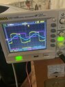
Your physical circuit will need a ground connection to protect the insulators, so install a real ground connection now, tell us where it is, and keep it in place. That is also a safety issue.

You are also going to need a protective ground when you use a comparator. If, as you say, the ground makes no difference to the 3:1 problem with your prototype, then why do you resist installing the protective ground now?

I learned, long ago, not to waste time diagnosing problems without a solid ground. I cannot diagnose your 3:1 problem, without a ground and a circuit diagram showing that ground.

imsmooth10 said:
When setting up the .trans command it seems that the Mac requires you to manually type in the values while the PC has a better interface. Is that correct?
I do not use Mac so I do not know. Mac costs too much and restricts the software I can run. LTspice has the same internal functionally. There are often several ways to edit something, by using mouse clicks while holding control keys.

imsmooth10 said:
Also, what is the deal with the currents going backwards unless I flip the components.
You have discovered that the reference current direction is terminal 1 of the component. It is an old and fundamental convention that, earlier, made SPICE possible. You will need to follow, or work around it. If it is a problem, flip the component, or place a unary negative sign in the specification, or the plot window trace equation.
 
  • #35
Do you have some design specs for input and output at each interface.

If a 100:1 impedance divider operates as 3:1 then you must have crosstalk.

Without an accurate schematic and layout of all components , your problem is unsolvable.
 
  • #36
Made a solid ground. Connected the divider. No difference and still wrong measurements. Then, as a guess I disconnected the p5205 differential probe and held it in the air. I was seeing the strange waveform.

Apparently, my probe has issues and I was never making a proper measurement. I switched probes and now I can see the proper phase shift. I'm still not seeing a 1:100 division, but it is better. I'm going to buy another probe.

I know the p5205 is no longer serviceable. Any suggestions for a good replacement. p5205a?
 
  • #37
imsmooth10 said:
Made a solid ground. Connected the divider.
I tried mind reading, but I am not doing well today, you are going to have to help me.
What or where did you ground something?
What sort of divider did you use?
How did you connect the divider?
Maybe it is time for you to use LTspice to draft an up-to-date circuit diagram. It does not have to run correctly.

If you change an LTspice.asc file to LTspice.asc.txt , you can attach it to a post, then others can run and edit it. That is the most compact way to communicate circuit diagrams clearly.

Do not post screenshots.
Alternatively, use the "Tools" menu, "copy bitmap to clipboard".
Save the image as a .png or .jpg
 
  • #38
imsmooth10 said:
I know the p5205 is no longer serviceable. Any suggestions for a good replacement. p5205a?
The Diff. Probe P2505 only has a CMRR of > 300 @ 100 kHz. or <-30dB error. So a good ground is essential on the signal with a short ground connection. Verify again with both inputs and gnd to gnd for a flat trace.

Probing the HV output will radiate EMI measurement problems beyond the scope of this thread. only use the C divider output.
You can improve it further with 100 pF\10 nF ( Z(f)= 212 Ohms @ 75kHz to probe.
 
  • #39
Baluncore said:
I tried mind reading, but I am not doing well today, you are going to have to help me.
What or where did you ground something?
What sort of divider did you use?
How did you connect the divider?
Maybe it is time for you to use LTspice to draft an up-to-date circuit diagram. It does not have to run correctly.

If you change an LTspice.asc file to LTspice.asc.txt , you can attach it to a post, then others can run and edit it. That is the most compact way to communicate circuit diagrams clearly.

Do not post screenshots.
Alternatively, use the "Tools" menu, "copy bitmap to clipboard".
Save the image as a .png or .jpg
Still learning how to use LTspice. Below is the LTSpice tank model. All these years I should have started using it. The tank is modeled pretty close to how mine works.
 

Attachments

  • #40
TonyStewart said:
Verify again with both inputs and gnd to gnd for a flat trace.

Probing the HV output will radiate EMI measurement problems beyond the scope of this thread. only use the C divider output.
You can improve it further with 100 pF\10 nF ( Z(f)= 212 Ohms @ 75kHz to probe.
You're saying to short the probe ends together or to test them on the grounding lead?

When you say only use the C divider output are you referring to a capacitative divider or something else?
 
  • #41
imsmooth10 said:
You're saying to short the probe ends together or to test them on the grounding lead?
YES by connecting both inputs to either signal and ground, you are measuring the CMRR and crosstalk. So expect it must be a flat line.

When you say only use the C divider output are you referring to a capacitative divider or something else?

YES and it's called "capacitive" and not capacitative.
 
  • #42
TonyStewart said:
YES by connecting both inputs to either signal and ground, you are measuring the CMRR and crosstalk. So expect it must be a flat line.

When you say only use the C divider output are you referring to a capacitative divider or something else?

YES and it's called "capacitive" and not capacitative.
When I connect both leads together they are picking up significant EMI when I power up my device. I suspect something is not working with the probes. Any suggestions to troubleshoot them or the power supply (1103)?
 
  • #43
imsmooth10 said:
When I connect both leads together they are picking up significant EMI when I power up my device. I suspect something is not working with the probes. Any suggestions to troubleshoot them or the power supply (1103)?
You will have to show a picture of everything with all power sources with schematic showing nodes, and sources of AC. SMPS (DC) are notorious for leakage of CM noise when isolated. Then we can analyze and fix.
 
  • #44
I can get there tomorrow and see what I can do. However, I just connected both probe ends to a ground wire and I do not get a flat line. When I power on a high frequency device nearby I see a high voltage signal on the scope. Not sure what else there is to show. Seems like something is broken.
 
  • #45
After switching to a standard probe I was able to get the correct values and waveforms using a resistor divider as well as a capacitor divider. Both worked as predicted.

The problem was with the differential probe and the noise overwhelming the signal. I am done with this thread and will try to address the probe issues in my other thread.
 
  • Like
Likes TonyStewart
  • #46
Edited LTspice schematic and plot files attached.
Includes notes on simulation, and a 101:1 voltage divider.
 

Attachments

  • #47
Baluncore said:
Edited LTspice schematic and plot files attached.
Includes notes on simulation, and a 101:1 voltage divider.
thanks for the edits. I have some questions now as I'm trying to learn how to use LTSpice.
1. How did you separate the "pulse" command from the voltage source. I tried to move it by I just moved everything. I hovered over to no avail.

2. Where did you get the "ferrite core" for the transformer and put it in-between L2 and L3? Did you just draw vertical wires? Doesn't the K1 command link the two inductors together so why do I need to draw the core or is it just aesthetics?

3. How does the wire connection at the bottom between L2 and L3 change the behavior from my original schematic? I can see when I remove it the voltages change.
4. How is setting the V(a) condition changing the analysis much other than setting the initial voltage to 240? Is it necessary? In reality, aren't both voltages really zero in the beginning?
4b. How did you enter the label "a"
5. what is the value of 7m15 and 20m? Is 20m 20mH? What is 7m15 then? 7.15mH?
6. How is the behavior of the voltage divider with the parallel capacitors different/better than just one or the other.
7. How do I open the .plt file for viewing?

I know it's a lot of questions and I appreciate your help.
 
Last edited by a moderator:
  • #48
1. How did you separate the "pulse" command from the voltage source. I tried to move it by I just moved everything. I hovered over to now avail.
Select the 'move' or 'drag' hand to select the text you want to move away from the source. I try to keep the head-end of the text under its voltage source, so I can find it and do not get confused with multiple sources.

2. Where did you get the "ferrite core" for the transformer and put it in-between L2 and L3
I drew it using isolated track segments. Iron cores get a couple of parallel tracks, or sometimes the rotated coupling coefficient text.

3. How does the wire connection between L2 and L3 change the behavior from my original schematic
It provides the required ground reference to the secondary side of the transformer. It does it in a way that shows it must be part of the connections. Don't forget that grounds between modules are all hidden connections.

4. .IC Va...which voltage is Va
.IC V(a) is the initial voltage on node a of the circuit = capacitor voltage relative to ground. I left the inductor current and flux at zero, but guessed the V(a)=240 to avoid the 0.5 second of simulation needed to get the voltage symmetrical about zero. I left the first couple of cycles showing during the transient analysis.

5. what is the value of 7m15 and 20m? Is 20m 20mH? What is 7m15 then?
The SI prefix takes the place of the decimal point. It is easier to read fast, or on a poorly printed circuit diagram.
20m = 20.0m = 20.0 mH = 0.02 H = 2e-2 H.
7m15 = 7.15m = 7.15 mH = 0.00715 H = 7.15e-3 H.
But never use the unit symbol as part of the value, or you will find that a 1F capacitor has a capacitance of only one femtofarad.
In SPICE, M is also milli, but avoid the use of upper-case M, except as the first letter of Meg = 1e6.

6. How is the behavior of the voltage divider with the parallel capacitors different/better than just one or the other.
The resistors maintain the DC which is important for a zero crossing detector or an oscilloscope. The capacitors give it the wide bandwidth required to avoid phase shifting fast signals. The parallel combination keeps the phase shift zero, and the frequency response flat, all the way from DC to daylight.

7. How do I open the .plt file for viewing?
When you 'Run' the simulation, LTspice uses it to generate the plot window traces and colours. It is written when you 'file', 'save plot settings'.
You can look inside using a text editor, but don't edit it by hand.
 
  • Informative
Likes berkeman
  • #49
imsmooth10 said:
4. How is setting the V(a) condition changing the analysis much other than setting the initial voltage to 240? Is it necessary? In reality, aren't both voltages really zero in the beginning?
When in LC resonance, current in the inductor is in quadrature with voltage on the capacitor, so they are never zero at the same time. If they both start the simulation at zero, it takes about 40,000 cycles of oscillation before the circulating energy builds up, and the voltage becomes symmetrical about zero. I avoid that simulation settling time, by starting the capacitor with a non-zero voltage.
It is like pulling a child back on a swing, then letting them go, to get things moving quickly.

imsmooth10 said:
4b. How did you enter the label "a"
Menu 'edit', 'Label Net'. Shortcut F4, or the 'Label Net' button in the toolbar, between the ground and resistor icons.
 
Last edited:
  • #50
Some imperfections to simulation may include:
- k coupling coefficient won't be exactly 1 and the leakage becomes the mutual inductance L4 a series fraction of primary inductance and dampens the resonance.
- V1 source must include RdsOn of FETs or added as a discrete R.
- L2 has no resistance but may be added by default settings for some L/R ratio.
- using 0 to 200V primary has the disadvantage of adding reducing L from saturation and +/-100 V removes that DC current offset.
 
  • #51
My goals is to get a good zero crossing trace for my capacitor voltage. I was able to get a good noise-free signal with an optocoupler I had lying around. The violet trace is the output when analyzing the capacitor voltage (not shown on the scope).

The problem is that I need a resistor to limit the maximum current to the LED to 25ma, which increases the voltage necessary to get the coupler to start detecting a lower voltage.

I'm trying to go through the data sheets on mouser and digikey to find one that has fast switching, low turn-on voltage, minimal propagation delay and a diode that can tolerate a higher current to give me the ability to detect a voltage ranging from 0-500Vrms.

Any suggestions for a good optocoupler/isolator?
 

Attachments

  • opto.jpg
    opto.jpg
    40.7 KB · Views: 97
  • #52
imsmooth10 said:
My goals is to get a good zero crossing trace for my capacitor voltage.
Why, or what will you use the signal for?
You need to write some specifications. How do you define "good" ?

An optocoupler and resistor is not the solution if you want a crisp edge at the right time. An optocoupler will always switch a few volts late, while resistor current will be lowest, just when you need it to be greatest, and greatest when you want it to be lowest.

There are many solutions, each with its own pros and cons.

It seems you do not want a pulse on crossing, but a square wave that is in phase with capacitor polarity. How close to in phase?
Do you require symmetry, or can the wave have a fast rising edge with a slower falling edge?
 
  • #54
I just seem to go deeper into the rabbit hole.

Baluncore, you are right. I don't want pulses on zero crossing, but a square wave that closely matches the polarity of the capacitor, Symmetry would be preferred.

Tony, the Falstad applet was really nice. I'm sure much of what I think is wrong so I am ready hear the right answer:

I thought the purpose of the isolator was so two dissimilar circuits could get "linked". The diode simply needs current from a closed loop to turn the other side on and off. Why does the left side of the circuit need to share a ground? Can't I run the left side with a non-grounded, floating sinusoidal voltage source?

Also,
1. What's the purpose of the schottky diode? When I delete it nothing seems to change.
2. What is the purpose of the 1M on top of the 100pF capacitor in parallel? You have capacitance 100:1 divider.How are you are picking the value of the resistor to go with the 100p capacitor?
 
Last edited by a moderator:
  • #55
The 100 pF was a current limiter voltage divider. The 1Meg and clamp diode were redundant for a unipolar signal 0 top 400V.

now I AC coupled reduced current to <4mA and phase shifted diode current 90 deg. The 10k senses current limited by the C reactance with some tiny fringe effects on duty cycle.

duty cycle is 50% +/-2 https://tinyurl.com/2pyrb6a2
 
  • #56
In both of your applets will the isolator's diode work when the AC source voltage is very low? I see it works on the simulation. The issue I was having was at low voltages there was not enough current to turn the isolator's diode on.

Also, the phase error addition aside, what is the functional difference between the two applet's output?
 
  • #57
When input current is low, you raise collector R value the same and buffer as I did. The diodes capacitance is not modelled so there are freq. limits and also tolerances on hFE are not an option there.

Often the opto losses are near the hFE gain so you see the CTR specs. are near 1 or worst case maybe 10% and best case >> 100% but the biggest variable in production is hFE. (depending on p/n)
 
  • #58
The diode, in antiparallel with the optocoupler LED, prevents destruction of the LED by reverse voltage.

The greatest slew-rate of the capacitor voltage is at the time of the zero-crossing. It would be sensible to use a capacitor to deliver the current needed to drive the optocoupler LED. The gating of that current through the optocoupler could be done by the capacitor voltage.
 
  • #59
Baluncore said:
The gating of that current through the optocoupler could be done by the capacitor voltage.
meaning:
Since I chose a small series C , its impedance being highest by far the 90 deg. Phase shift is dominated by Vc drop and < 1% by load= Vf/If +Rs, so the phase error is low.

Since the largest voltage drop is across C and current sensed by the real R (albeit nonlinear diode effect, it is still real R. for the most part neglecting low current diode capacitance)

In the initial divider we had matched R1C1 to R2C2 to get a wide spectrum voltage divider rather than the familiar partial derivative frequency response.
 
  • #60
TonyStewart said:
When input current is low, you raise collector R value the same and buffer as I did. The diodes capacitance is not modelled so there are freq. limits and also tolerances on hFE are not an option there.
You're referring to the 10k resistor as the current sense, right?. If the voltage goes up on the cathode side of the LED diode doesn't that decrease the voltage drop across the diode and hence the current driving it? When you say "raise" the collector R are you saying you choose different design values? My issue is the voltage source varies from 0 to 500Vrms and the value of R would be fixed.
 
Last edited by a moderator:

Similar threads

  • · Replies 32 ·
2
Replies
32
Views
3K
Replies
15
Views
2K
Replies
38
Views
6K
Replies
20
Views
4K
Replies
14
Views
5K
  • · Replies 27 ·
Replies
27
Views
3K
  • · Replies 22 ·
Replies
22
Views
4K
Replies
14
Views
8K
Replies
6
Views
3K
  • · Replies 16 ·
Replies
16
Views
2K