Troubleshooting Gated D Latch Waveforms

  • Thread starter Thread starter perplexabot
  • Start date Start date
  • Tags Tags
    Schematic
AI Thread Summary
The discussion revolves around troubleshooting a gated D latch circuit where the output waveform behaves unexpectedly, changing state incorrectly. The user suspects issues related to transistor sizing or connections, particularly with power and ground nodes. Suggestions include checking for incorrect connections and ensuring that the QN node is not grounded, as it should be floating or connected to a small capacitor. The conversation highlights the importance of proper test bench setup and circuit biasing in achieving accurate simulation results. Overall, the user seeks assistance in identifying the cause of the waveform anomalies.
perplexabot
Gold Member
Messages
328
Reaction score
5
Hello all. So I finished making a gated D latch. I used the Analog Environment to plot the waveforms. I have provided the schematic and the waveforms below.

The output is kind of weird, as you will see.

Thank you for reading.
EDIT: Been trying to figure out what the problem is for a while now, still don't know what it could be. Could it have to do with transistor sizing? I did the same circuit on my phone (using an app called EasyCircuit) and I believe the correct waveforms were achieved. I have no idea what may be causing the output to change state (in the case of the image shown, the output changes at the rising edge, as it should, but then changes on the falling edge too! [which it should not, because the input didn't change!]). What may be causing this peculiar event? I hate going to sleep like this, but it looks like I have no choice. If anyone has any suggestions, anything at all! Please send them my way. Thanks again. I will reply after I wake up (assuming I get replies.)
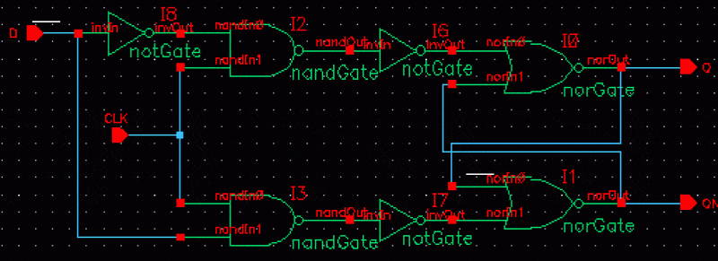
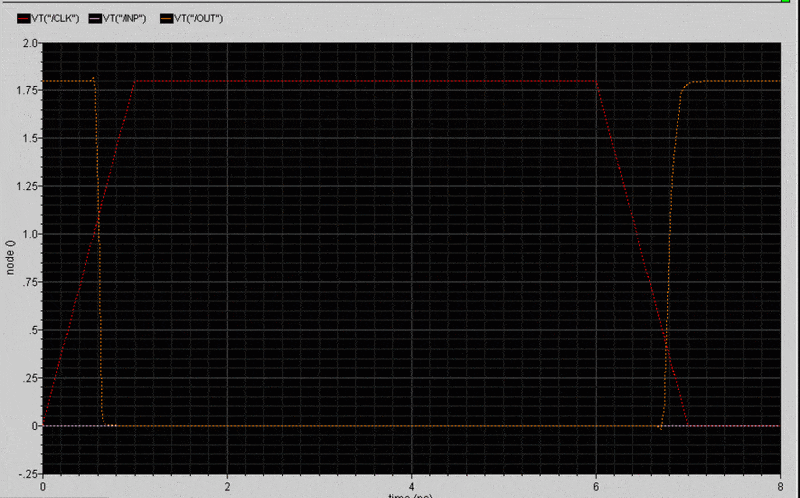
latch_schem.gif

waveforms.gif
 
Last edited:
Engineering news on Phys.org
The labels on your simulation output do not correspond to your schematic. Does INP = D and OUT = Q.

This is indeed strange. I suspect you have a missed/screwed up inherited connection (power/ground/substrate) somewhere.

Can you check all your inherited connections then look at every single node until you find one that doesn't make sense?

Good luck!
 
  • Like
Likes 1 person
analogdesign said:
The labels on your simulation output do not correspond to your schematic. Does INP = D and OUT = Q.

This is indeed strange. I suspect you have a missed/screwed up inherited connection (power/ground/substrate) somewhere.

Can you check all your inherited connections then look at every single node until you find one that doesn't make sense?

Good luck!

The reason for that is because I created a symbol for the D-Latch and then used that in a new schematic. Sorry, I should have stated that. Here is a screenshot. Thank you for the reply and help.

EDIT1: I am not so sure what you mean by "inherited connections," but I double checked the vdd!'s and gnd!'s for the nand, not and nor gates. I was not able to find anything strange.
EDIT2: Triple checking nodes as you have suggested, I can see a vdd supply net connected to a node that is called vdd! and not vdd. Is this a problem? I am assuming this is as it should be.

PS: Anyone have a clue? Please this is really bugging me!

true_schem.gif
 
Last edited:
The problem is QN. It should be floating rather than grounded. You can either leave the QN node open or you can connect it to a very small capacitor.
 
  • Like
Likes 1 person
analogdesign said:
The problem is QN. It should be floating rather than grounded. You can either leave the QN node open or you can connect it to a very small capacitor.

I just want to say, "I love you!"
 
perplexabot said:
I just want to say, "I love you!"

Ha ha, no problem! In my experience 95% of all really weird simulation results are due to how we set up the test bench or have biased or connected the circuit.
 
analogdesign said:
Ha ha, no problem! In my experience 95% of all really weird simulation results are due to how we set up the test bench or have biased or connected the circuit.

Thank you for your (wonderful) help and interesting information.
 
Back
Top