What is happening to the PN, NP, and MS junctions when using a BJT?

  • Thread starter CraigH
  • Start date
  • Tags
    Bjt
In summary, current can flow between the base and collector when a voltage is applied between these terminals. This is because the depletion regions which originally stopped the current from flowing have shrunk.
  • #1
CraigH
222
1
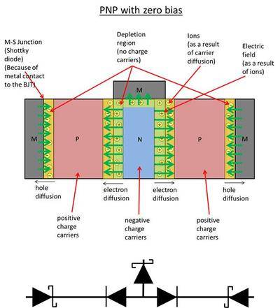
With no external voltage applied there exists an insulating depletion region between all of the junctions of dissimilar materials. This is formed when the dissimilar materials first contact: the free carriers in one material (either positive or negative) diffuse into the second material and recombine with an opposite carrier. Since the free carriers have crossed the junction the dopants (e.g phosphorus & boron) which these carriers originally belonged to become ionised. This creates electric fields which prevent further diffusion. This area of ions is void of free carriers, and is thus an insulator. This insulating layer is known as the depletion region.

The electric fields (shown by green arrows) in a BJT with no external voltage are shown below:
DKdPlqx.jpg
This is the part I don't understand

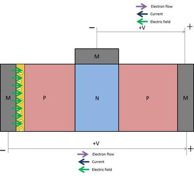
However, if a voltage is applied between the base-emitter and collector-emitter terminals, a current can flow between these terminals. But why? what has happened to the depletion regions which originally stopped the current from flowing?

Thanks!
fc4C46m.jpg
 
Last edited:
Engineering news on Phys.org
  • #2
Depletion regions shrink and conduct when they are forward biased. Normally, they expand and block current (up to a point) when they are reverse biased.

When you forward bias the base-emitter junction the B-E depletion region shrinks until current begins to flows. This brings holes and electrons into the base. The base-collector depletion region is still there because it is reversed biased when the BJT is in triode or saturation mode. It has a real voltage and electric field. Charge carriers brought into the base by the B-E current will diffuse towards the B-C junction and get swept across by the electric field if they have the right sign.

In short, if you inject current across the base and emitter, a larger current will get swept across from Emitter to Base to Collector.

A picture is worth a thousand words. Someone made a nice looking wiki which goes into detail and has graphs which are really needed to understand how BJT's work. You can find it here.
 

1. What is the role of a BJT in the PN, NP, and MS junctions?

A BJT, or bipolar junction transistor, is a type of semiconductor device that is used to control the flow of current in a circuit. In the PN junction, the BJT acts as a switch, allowing or blocking the flow of current between the two layers of the transistor. In the NP junction, the BJT acts as an amplifier, amplifying the current flowing through the transistor. In the MS junction, the BJT acts as a diode, allowing current to flow in one direction but not the other.

2. How does a BJT affect the conductivity of the PN, NP, and MS junctions?

A BJT can affect the conductivity of the PN junction by controlling the base current, which in turn controls the amount of current that can flow through the transistor. In the NP junction, the BJT can amplify the conductivity of the transistor by increasing the amount of current flowing through it. In the MS junction, the BJT can control the direction of current flow by acting as a diode.

3. What causes the PN, NP, and MS junctions to break down when using a BJT?

The PN, NP, and MS junctions can break down when using a BJT due to excessive current flow or voltage. When the current or voltage exceeds the threshold levels, the junctions can become damaged and lose their ability to properly control or amplify current. This is known as junction breakdown and can lead to failure of the BJT and the circuit as a whole.

4. How does temperature affect the performance of the PN, NP, and MS junctions when using a BJT?

Temperature can have a significant impact on the performance of the PN, NP, and MS junctions when using a BJT. Higher temperatures can cause an increase in the leakage current of the transistor, leading to decreased performance and potential breakdown of the junctions. Additionally, temperature can affect the mobility of the charge carriers, altering the conductivity of the transistor.

5. What are the main differences between the PN, NP, and MS junctions in a BJT?

The PN, NP, and MS junctions in a BJT have different roles and functions. The PN junction acts as a switch, the NP junction acts as an amplifier, and the MS junction acts as a diode. Additionally, the doping levels and polarity of the layers in the junctions differ, resulting in different conductivity and current control capabilities. The PN junction has a higher doping concentration in the emitter and collector layers, while the NP junction has a higher concentration in the base layer. The MS junction has a single layer with a different doping concentration, resulting in different conductivity compared to the other junctions.

Similar threads

Replies
3
Views
751
Replies
5
Views
2K
  • Electrical Engineering
Replies
12
Views
1K
Replies
1
Views
790
  • Electrical Engineering
Replies
10
Views
2K
Replies
3
Views
2K
  • Electrical Engineering
Replies
6
Views
3K
  • Electrical Engineering
2
Replies
42
Views
8K
Replies
2
Views
4K
  • Atomic and Condensed Matter
Replies
2
Views
2K
Back
Top