Equation for BJT voltage controlled amplifier

AI Thread Summary
The discussion focuses on modeling the behavior of a BJT transistor used as a voltage-controlled amplifier (VCA) in a synthesizer project. The original assumption that the output voltage V_e(t) could be modeled as the product of the control voltage V_b(t) and the input voltage V_c(t) is incorrect, as this does not account for the transistor's current relationships. Participants suggest using the hybrid pi equivalent model to accurately represent the transistor's behavior, emphasizing the importance of resistor values and transistor parameters in the calculations. The circuit's complexity is acknowledged, with discussions about its application in generating sound effects, specifically a rim-shot in electronic drums. The user is encouraged to explore further and refine their model based on feedback and additional circuit analysis.
kvtb
Messages
11
Reaction score
0
Hi,
as mentioned in my previous thread, I'm currently busy with a 'small' project of translating an analog device (synthesizer, based on schematics) into a digital (software) version.

I know 'nothing' about EE, I'm a Computer Science guy, so hopefully this question is not too easy :-)

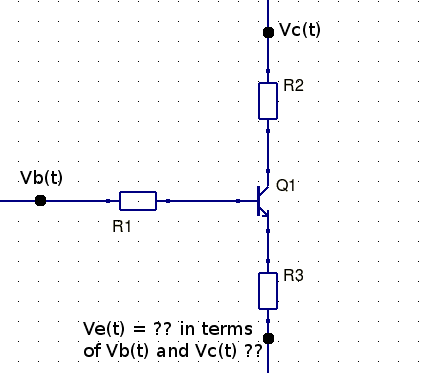
This question is about how to model the behaviour of a transistor. In the analog device, a single transistor is used as a voltage controlled amplifier.
- The control voltage envelope V_b(t) enters via the base of the transistor,
- the voltage to be shaped according to the envelope V_c(t), enters via the collector
- the output is a voltage V_e(t) of which was until now modeled as simply V_e(t) = V_b(t) \cdot V_c(t)However... later I noticed that every website about transistors say that I_e = I_b + I_c, so that would imply that it is impossible to get V_e(t) = V_b(t) \cdot V_c(t)So, my question is simply,
- given a control voltage as function of time V_b(t)
- given an input voltage V_c(t)

attachment.php?attachmentid=23532&stc=1&d=1265308751.png
How do I calculate V_e(t) in terms of V_b(t), V_c(t), R1, R2, R3 and any transistor dependent constants?

Thanks in advance!
 

Attachments

  • emittervoltage.png
    emittervoltage.png
    2.5 KB · Views: 1,045
Engineering news on Phys.org
Even if Vb and Vc are derived from ideal voltage sources, you cannot just dangle Ve like that. (Well, you "can", but I don't think that the transistor would do anything. I don't know what would happen, actually.) For instance, perhaps there is another resistor (i.e. a load) connected from Ve to ground?

BTW, what kind of transistor is it? The symbol that you have used suggests npn, perhaps 2222.
 
kvtb said:
Hi,
as mentioned in my previous thread, I'm currently busy with a 'small' project of translating an analog device (synthesizer, based on schematics) into a digital (software) version.

I know 'nothing' about EE, I'm a Computer Science guy, so hopefully this question is not too easy :-)

This question is about how to model the behaviour of a transistor. In the analog device, a single transistor is used as a voltage controlled amplifier.
- The control voltage envelope V_b(t) enters via the base of the transistor,
- the voltage to be shaped according to the envelope V_c(t), enters via the collector
- the output is a voltage V_e(t) of which was until now modeled as simply V_e(t) = V_b(t) \cdot V_c(t)

However... later I noticed that every website about transistors say that I_e = I_b + I_c, so that would imply that it is impossible to get V_e(t) = V_b(t) \cdot V_c(t)


So, my question is simply,
- given a control voltage as function of time V_b(t)
- given an input voltage V_c(t)

attachment.php?attachmentid=23532&stc=1&d=1265308751.png


How do I calculate V_e(t) in terms of V_b(t), V_c(t), R1, R2, R3 and any transistor dependent constants?

Thanks in advance!

The 1st equation highlighted in bold is dimensionally inconsistent. You cannot multiply 2 voltages and get a voltage. Are you trying to perform an analog multiplication of 2 signals? There are circuits that do that. I would search "analog multiplier" or "Gilbert multiplier".

The 2nd bold highlight can be answered as follows. By "Ve", I presume you mean the emitter potential with respect to ground. Look up the "hybrid pi equivalent" model of the bjt operating in small signal mode. The bjt parameters are "r_pi, hfe, & gm or re". Also, r_pi = hfe/gm, where gm = Ic/Vt, Vt = kT/q. You can then compute the ac gain, i.e., Ve will be a function of Vb, the resistor values, and bjt properties. Selecting the right values for the R's minimizes the bjt parameters' influence on circuit behavior.

Did I help? A good reference text will answer your questions in detail. Horowitz is a good text.

Claude
 
turin, cabraham, thanks for your replies.

I think my question was perhaps not clear or incomplete:

turin: The schematic is just a small part of a larger schematic to illustrate my question, that's why there's no ground.
If you interested, please take a look at transistor Q65 in cell J8 of this schematic:
http://www.kolumbus.fi/janne.husu/specs/909vb.gif
The transistor in question is a 2SC2603-F (no longer in production - but the datasheets are available)

cabraham: I do not try to do (analog) multiplication of two voltages. In the software model I'm building, I incorrectly assumed that the behaviour of a transistor VCA could be approached by multiplying the envelope signal (at base) with the input signal (at collector).

I will look into the hybrid pi equivalent model to see if I can use it to model the behaviour of a single-transistor VCA.

Thanks again for your help.
 
Last edited by a moderator:
Looks like Q65 is just gating through noise from the diodes D91 and D92 with a decay envelope. Hence the rim-shot. I may be wrong however.
 
kvtb said:
... I do not try to do (analog) multiplication of two voltages. In the software model I'm building, I incorrectly assumed that the behaviour of a transistor VCA could be approached by multiplying the envelope signal (at base) with the input signal (at collector).
What's the difference? What's VCA? Anyway, that is certainly not the behavior of Ve given Vb and Vc.

BTW, the model of the transistor can be very dependent on 1) the type that you are using, and 2) the surrounding circuit connections to the three electrodes. For example, hybrid-π model may or may not be applicable. (Hybrid-π model is a small-signal model, correct?) I haven't looked at your schematic yet. I'll let you know if I can figure out what the transistor is supposed to do.

dlgoff said:
Looks like Q65 is just gating through noise from the diodes D91 and D92 with a decay envelope. Hence the rim-shot.
What's a rim-shot? I've never heard of such a circuit. Is this some sort of musical circuit? (wikipedia says that a rimshot is a drumming technique.)

EDIT:
Upon cursory inspection, here's how I visualize your transistor circuit:

Firstly, it can be reduced no further than:
Q65, D91, D92, R408, R415, R417, R418, R423

It has three input voltages (ultimately for collector control) and one input current (base), and it produces one output current (emitter).

The three input voltages come from three op-amps? and are presented at the three resistors: R408, R415, and R417. The three currents feed into the voltage divider circuit of R418 and R423, but the maximum input voltage to this divider is clamped by the diode circuit of D91 and D92. (Is that the right term - "clamped"?). The output of the voltage divider provides a Vc at your transistor.

Since the emitter is connected directly to a negative op-amp? input, the positive op-amp? input is grounded, and the op-amp? has negative feedback, the emitter voltage is held at 0 V.

So, the three input voltages basically control Vce (subject to the diode clamp constraint), without negative emitter feedback. The output of the transistor is a current output that flows through the op-amp? feedback RC circuit.

With the given Vce, the output current is basically determined by the input current at the base. This current comes from Q64 through two resistors: R401 and R403. I think that these resistors are mainly for filtering and feedback to Q64.

So, this looks like a base-to-emitter current amplifier circuit that is somehow controlled by three voltages (which somehow work together to determine the current amplification by controlling Vce). I don't know if the diode circuit is just for protection, or if it has a functional purpose.
 
Last edited:
turin said:
What's a rim-shot? I've never heard of such a circuit. Is this some sort of musical circuit? (wikipedia says that a rimshot is a drumming technique.)
The circuit looks to be an electronic drum (percussion) set. It looked like the diodes were involved in making the noise (used to simulate snare durms) but I'm not sure since there is also a "noise section" in the circuit. Here is a way to generate and amplify thermal noise from a diode:
broadband-noise-generator-circuit.gif

D1 generates noise,...
http://www.simplecircuitdiagram.com/2009/12/25/broadband-noise-generator/"

The three wave forms, F1, F2 and F3 are the envelopes used to modulate the noise. Which makes the sound of a rim-shot. i.e. the stick strikes the head and rim of the snare drum at the same time.
 
Last edited by a moderator:
dlgoff, turin, thanks for your replies.

let me try to explain the circuit in the link I've given, using another link;
http://mitglied.multimania.de/raf909/rimshot.htm

the three op-amps and surrounding capacitors and resistors are sine wave generators, these generate a sine wave (at three different frequencies) with different damping.

the three sines are then mixed together, and 'wave shaped': the two diodes are 'limiting' the amplitude of the mixed signal.
(In other parts of this schematic, you'll also see this construction with these two diodes. For example, to 'translate' a triangle wave into a 'sine' wave. So these diodes are not related to noise generation).

For those who have LTspice installed, and are interested in the output of the Rimshot circuit, please load and simulate the attached file. In the LTSpice file, you'll see transistor Q3, which is the transistor that does the VCA.

You may want to 'probe' the following nets:
F1, F2, F2 (to see the sine waves)
shaped (effect of the two diodes, and input to the collector of the transistor)
ENV ( the envelope applied to the base of the transistor)
 

Attachments

Last edited by a moderator:
So these diodes are not related to noise generation
I stand corrected.
 
  • #10
Can you describe the "trigger"? I'm most curious about the amplitude of the trigger (above ground). I imagine that it is just a quick square voltage pulse of several volts amplitude (above ground) that is produced by a key press or something. I don't want to know where it comes from, just what are its expected characteristics.
 
  • #11
Hi, the trig signal is a +5V pulse, duration is 2 msBTW, in mean while, I've tried to 'measure' a transfer function (as function of Vb and Vc) and tried to fit an equation on top of it. I'll post results later.
 
  • #12
OK. That's what I expected. I don't think I can offer any further input.
 

Similar threads

Back
Top