Estimating the upper 3dB cutoff in a MOSFET amplifier

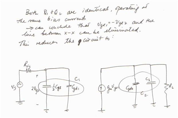
In summary, the conversation discusses methods for estimating the upper cutoff frequency using the open circuit time constant method. The second picture shown is a simplified version of the first, where the drain of Q2 becomes grounded and the GS capacitors combine to half of their original value. The conversation also mentions the use of a 1V test voltage to find equivalent resistances and the concept of removing redundant wires in a circuit.
  • #1
Forcefedglas
26
0
Homework Statement
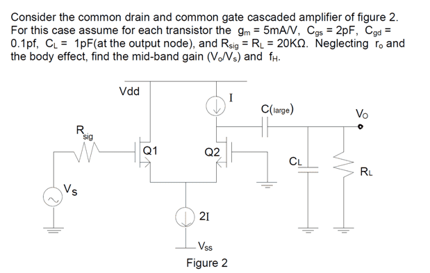
fUH2nU7.png

I've found the gain, but now I need to estimate the upper cutoff frequency with the open circuit time constant method, so the upper 3dB cutoff would roughly be $$\sum_{i = 1}^{n} \frac{1}{\tau_i}$$

The attempt at a solution
I'm currently trying to make sense of the given solutions:
1xSwCpR.png
IDhXnex.png


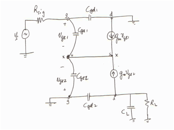
I got something similar to the first picture after drawing out the small signal equivalent, but I'm completely lost as to how they went from that circuit to the one in the second picture. Why does the drain of Q2 suddenly become grounded, and how did the GS capacitors combine and turn into half of their original value? I've tried searching around but haven't found any explanations of the simplification method used here.

I attempted to use a 1v test voltage at the gate source capacitors (in the first circuit) to find the equivalent resistance seen by them but that yielded a different answer to what I get if I work it out via the second circuit.

Any help/tips would be greatly appreciated, thanks.
 
Physics news on Phys.org
  • #2
It might help to split apart (graphically) some of the ground connection in order to visually isolate in the input and output portions of the circuit. So starting with their first picture and breaking up the ground connections at the drain of Q1 and the gate of Q2:
upload_2016-9-27_7-30-33.png
 
  • #3
gneill said:
It might help to split apart (graphically) some of the ground connection in order to visually isolate in the input and output portions of the circuit. So starting with their first picture and breaking up the ground connections at the drain of Q1 and the gate of Q2:
View attachment 106562

Ah ok, so the equivalent capacitances (and the voltages across them) combine and since Vgs2=-Vgs1, the current sources are equivalent and one can be removed? So whenever there's a wire connecting two portions of a node like this, can you always just remove it and proceed to simplify the circuit? I guess I'm slightly confused as to what happens to the s1-s2 wire and in what situations I can effectively remove it.

I have one more question, the equivalent resistance seen by 1/2Cgs is Rsig=20k, so the time constant is 20nS. Shouldn't I be able to get the same answer if I insert a test voltage of 1V and sum the equivalent resistances seen by Cgs1 and Cgs2 on the first circuit diagram? When I try to do it however, I get this for the equivalent resistance seen by Cgs1 (other capacitors opened, 1v test voltage where Cgs1 is):
NHFwXKy.png

Which can't be correct as the time constant will already be larger than 20nS from Cgs1 alone. I calculated the equivalent resistance for Cgs2 as 100 ohms, so theoretically Req seen by Cgs1 should be 9.9k, however I've stared at this for hours and couldn't find any errors.
 
Last edited:
  • #4
Forcefedglas said:
Ah ok, so the equivalent capacitances (and the voltages across them) combine and since Vgs2=-Vgs1, the current sources are equivalent and one can be removed?
More precisely, one is redundant since they are both producing the same current in the same direction.
So whenever there's a wire connecting two portions of a node like this, can you always just remove it and proceed to simplify the circuit?

I guess I'm slightly confused as to what happens to the s1-s2 wire and in what situations I can effectively remove it.

Usually the argument goes that if two nodes are at the same potential then connecting them with a wire will make no change in circuit operation (as no current will flow through that wire and no potentials will change as a result). Here there's an existing wire and the argument is reversed: removing the wire will not change the potentials at the nodes since Vgs1 = Vgs2.

I'll have to think about your test voltage setup.
 
  • #5
gneill said:
More precisely, one is redundant since they are both producing the same current in the same direction.Usually the argument goes that if two nodes are at the same potential then connecting them with a wire will make no change in circuit operation (as no current will flow through that wire and no potentials will change as a result). Here there's an existing wire and the argument is reversed: removing the wire will not change the potentials at the nodes since Vgs1 = Vgs2.

I'll have to think about your test voltage setup.

Thanks that clears up a lot, strange that I never specifically heard about this in any of my introductory circuit courses but it makes sense now.
 
  • #6
Forcefedglas said:
Thanks that clears up a lot, strange that I never specifically heard about this in any of my introductory circuit courses but it makes sense now.
You may have seen it used when simplifying highly symmetric resistance or capacitance networks. It's often seen as a simplification "trick" in puzzle or challenge type questions.
 

1. What is the purpose of estimating the upper 3dB cutoff in a MOSFET amplifier?

The upper 3dB cutoff is an important parameter in determining the overall performance and bandwidth of a MOSFET amplifier. It represents the frequency at which the signal output is reduced by 3dB, and serves as an indicator of the amplifier's ability to amplify high frequency signals.

2. How is the upper 3dB cutoff calculated for a MOSFET amplifier?

The upper 3dB cutoff can be estimated by analyzing the MOSFET amplifier's frequency response curve. It is typically measured by finding the frequency at which the signal amplitude is reduced by 3dB from its maximum value.

3. What factors can affect the upper 3dB cutoff in a MOSFET amplifier?

There are several factors that can affect the upper 3dB cutoff in a MOSFET amplifier, including the type and quality of the MOSFET transistor, the amplifier's input and output capacitance, and the amplifier's biasing and circuit design.

4. How can the upper 3dB cutoff be improved in a MOSFET amplifier?

To improve the upper 3dB cutoff in a MOSFET amplifier, one can use higher quality MOSFET transistors with better frequency response, minimize input and output capacitance, and optimize the amplifier's biasing and circuit design for high frequency performance.

5. Why is it important to accurately estimate the upper 3dB cutoff in a MOSFET amplifier?

Accurately estimating the upper 3dB cutoff is crucial for ensuring the desired performance and bandwidth of a MOSFET amplifier. It can also help in troubleshooting and optimizing the amplifier's design for specific applications.

Similar threads

  • Engineering and Comp Sci Homework Help
Replies
0
Views
511
  • Engineering and Comp Sci Homework Help
Replies
5
Views
3K
  • Engineering and Comp Sci Homework Help
Replies
8
Views
778
  • Engineering and Comp Sci Homework Help
Replies
2
Views
2K
  • Engineering and Comp Sci Homework Help
Replies
1
Views
1K
  • Engineering and Comp Sci Homework Help
Replies
6
Views
1K
  • Engineering and Comp Sci Homework Help
Replies
13
Views
2K
  • Engineering and Comp Sci Homework Help
Replies
29
Views
4K
  • Engineering and Comp Sci Homework Help
Replies
2
Views
967
  • Engineering and Comp Sci Homework Help
Replies
2
Views
1K
Back
Top