Analyzing this operational amplifier circuit with DC

  • #1
ZoeDale
11
1
Homework Statement
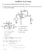
a) Treat the operational amplifier in the circuit below as ideal and solve for Vo.
b) Treat the op amp as a non-ideal device that is powered by VCC and VEE; describe several ways in which your answer in part a) will change.
Relevant Equations
KVL; KCL;
Hi all, I attached my attempt at a solution in the attached picture. I am using the textbook titiled as ”electronic circuit analysis“ by David E. Johnson, and op amp is in chap 3;
while I did not find any example that attach the Vee and Vcc with amplifier . It seems that v+ = v- doesn’t hold in this scenario; can anybody give me some hints?

thanks!
 

Attachments

  • IMG_3132.jpeg
    IMG_3132.jpeg
    27.5 KB · Views: 26
Last edited:
  • Skeptical
Likes berkeman
Physics news on Phys.org
  • #2
IMG_3132.jpeg
 
  • #3
Um, that circuit has a fundamental problem, and is non-physical. SPICE, for example, would throw an error if you tried to analyze it. Are you sure this came from a textbook?
 
  • #4
this is a problem from our qualify exam samples for practice. No solutions provided. :cry:
 
  • #5
ZoeDale said:
this is a problem from our qualify exam samples TAT for practice. No solutions provided.
Well, that circuit is complete nonsense as drawn, so there is no solution to the problem. Maybe that is the test of the problem -- you are supposed to reply that the circuit is nonsense in order to get credit.

Can you say what is totally wrong about that circuit?

1701990267207.png
 
  • #6
berkeman said:
Um, that circuit has a fundamental problem, and is non-physical. SPICE, for example, would throw an error if you tried to analyze it. Are you sure this came from a textbook?
Seems that v+ can not be equal to v- in the ideal condition; or the non-ideal condition. But I can not figure out what will happen in the circuit; Can you give more hints on that? Thank you!
 
  • #7
ZoeDale said:
Can you give more hints on that?
Opamp inputs must have some DC bias connection to somewhere to supply their input bias currents and to set the DC operating point. Do you see the issue now? :smile:
 
  • #8
berkeman said:
Opamp inputs must have some DC bias connection to somewhere to supply their input bias currents and to set the DC operating point. Do you see the issue now? :smile:
oh, you mean they should be on each side of the lying triangle's waist, separately?
 
  • #9
ZoeDale said:
oh, you mean they should be on each side of the lying triangle's waist, separately?
Sorry, I don't understand your response.
 

1. How do I calculate the DC gain of an operational amplifier circuit?

To calculate the DC gain of an operational amplifier circuit, you can use the formula: DC gain = -Rf/Rin, where Rf is the feedback resistor and Rin is the input resistor. Simply plug in the values of these resistors to find the DC gain.

2. What is the input offset voltage of an operational amplifier circuit?

The input offset voltage of an operational amplifier circuit is the voltage required at the input to bring the output voltage to zero. It is typically a small voltage value that can affect the accuracy of the circuit's output.

3. How do I analyze the input bias current of an operational amplifier circuit?

To analyze the input bias current of an operational amplifier circuit, you can calculate the current flowing into the input terminals of the op-amp. This current can cause voltage drops across resistors in the circuit, affecting the overall performance.

4. What is the common-mode rejection ratio (CMRR) of an operational amplifier circuit?

The common-mode rejection ratio (CMRR) of an operational amplifier circuit is a measure of its ability to reject common-mode signals. It is calculated as the ratio of the differential gain to the common-mode gain, and a higher CMRR indicates better rejection of unwanted signals.

5. How can I minimize offset voltage in an operational amplifier circuit?

To minimize offset voltage in an operational amplifier circuit, you can use techniques such as adjusting the input offset null pins, selecting precision resistors, or using chopper-stabilized op-amps. These methods can help reduce the impact of offset voltage on the circuit's performance.

Similar threads

  • Engineering and Comp Sci Homework Help
Replies
8
Views
1K
  • Engineering and Comp Sci Homework Help
Replies
34
Views
2K
  • Engineering and Comp Sci Homework Help
Replies
1
Views
1K
  • Engineering and Comp Sci Homework Help
Replies
18
Views
2K
  • Engineering and Comp Sci Homework Help
Replies
4
Views
2K
  • Engineering and Comp Sci Homework Help
Replies
4
Views
2K
  • Engineering and Comp Sci Homework Help
Replies
2
Views
2K
  • Engineering and Comp Sci Homework Help
Replies
0
Views
522
  • Engineering and Comp Sci Homework Help
Replies
18
Views
2K
  • Engineering and Comp Sci Homework Help
2
Replies
44
Views
3K
Back
Top