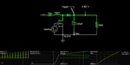
What is the issue with my boost converter design and how can I fix it?

In summary: It assumes a fixed load current. 2) For big voltage ratios, a transformer would be used in place of the inductor. That can reduce peak currents on the supply and load. 3) If the output load goes open circuit, the output capacitors will be damaged by overvoltage. 4) You need a controller with some feedback of output voltage to the regulator. That controller should limit the inductor current when there is a short circuit. A flyback converter uses a switch to turn on and off a transformer to change the voltage across the input and output capacitors. In summary, the converter does not change the duty cycle of the output.
  • #36
TonyStewart said:
These problems can be found simply by looking what fails when so much power is being pumped by examining the impedance and energy (heat) in every part with limits on peak and RMS current specs.
I really don't think there is a problem with the magnitude of the current.

L = 10 uH; V = 12 volt; f = 300 kHz; Duty = 30%.
Tcycle = 3.333 usec; Ton = 1 usec; Toff = 2.333 usec.

When the switch closes, the inductor is connected across the 12 V supply.
V = L·di/dt; ∴ di/dt = V/L = 12 V / 10 uH = 1.2 amp per microsecond.

With a 1 mA load current, it will take almost 1 msec for the output to rise to about 160 volts.
 
Engineering news on Phys.org
  • #37
Baluncore said:
I really don't think there is a problem with the magnitude of the current.

L = 10 uH; V = 12 volt; f = 300 kHz; Duty = 30%.
Tcycle = 3.333 usec; Ton = 1 usec; Toff = 2.333 usec.

When the switch closes, the inductor is connected across the 12 V supply.
V = L·di/dt; ∴ di/dt = V/L = 12 V / 10 uH = 1.2 amp per microsecond.

With a 1 mA load current, it will take almost 1 msec for the output to rise to about 160 volts.
When the switch opens, the inductor current does not stop and thus accumulates every cycle,;

1.2A, 2.4A, 3.6A, 4.8A, 6.0A, .. when does it peak? about half a cycle later at the LC resonance ~ 2.5kHz about 200 us !!!

The ideal solution , I believe is the autotransformer at the piezo resonance with AC using a forward regulator with feedback. ie. NFET primary switching at 50% with turns ratio to open circuit secondary voltage. i.e. not a flyback.
 
  • #38
TonyStewart said:
When the switch opens, the inductor current does not stop and thus accumulates every cycle,;
Negative. When the switch opens, the inductor voltage is reversed as it dumps the current through the diode, into the reservoir capacitor. Since the voltage during flyback is reversed, di/dt is negative, so the current falls rapidly to and through zero, then rings or oscillates a bit while waiting for the next Ton, during which the current rises again from near zero, to 1.2 amps.
 
  • Like
Likes DaveE
  • #40
core7916 said:
i am not getting meaning for current pump
A similar way of saying this is that your converter is operating in discontinuous conduction mode (DCM) because of the very low load current. So, the DC gain won't be ##\frac{1}{1-D}##, that is for continuous conduction mode (CCM).

I suspect you also have other implementation problems. But first, you must study some of the theory behind these circuits. You probably won't succeed with guessing, nor are we likely to make it work in your lab with occasional social media comments.
 
  • #41
Baluncore said:
Negative. When the switch opens, the inductor voltage is reversed as it dumps the current through the diode, into the reservoir capacitor. Since the voltage during flyback is reversed, di/dt is negative, so the current falls rapidly to and through zero, then rings or oscillates a bit while waiting for the next Ton, during which the current rises again from near zero, to 1.2 amps.
Please Read again. I meant the inductor current in the inductor will not stop ( for 200 us until it peaks due to resonance) . It will accumulate and the L/R=Tau >> dt so it WILL not decay as I said before.
 
  • Skeptical
Likes DaveE
  • #42
TonyStewart said:
I meant the inductor current in the inductor will not stop ( for 200 us until it peaks due to resonance) . It will accumulate and the L/R=Tau >> dt so it WILL not decay as I said before.
That is not what LTspice simulation shows.
The 30% duty cycle at 12 volts, and the much higher negative voltage during flyback, guarantees the inductor current reaches zero very rapidly.
I think you must be assuming the duty cycle is close to 95%, so there is insufficient time for flyback to complete before the next Ton starts.
 
  • Informative
Likes berkeman
  • #43
No I used <=50% d.f.

If you turn off the FET at startup, then read the max. voltage output , that overshoot will tell me what Q you chose from LC parts. (step response)

Step Overshoot = ?


Idc startup = Vin/(DCR+Rs+ESR)
What is your max current?

i.e. if startup is CCM there may be problems with inductor saturation from excess current.
 
Last edited:
  • #44
TonyStewart said:
No I used <=50% d.f.

If you turn off the FET at startup, then read the max. voltage output , that overshoot will tell me what Q you chose from LC parts. (step response)

Step Overshoot = ?


Idc startup = Vin/(DCR+Rs+ESR)
What is your max current?
This is not a resonant or quasi-resonant design. It is a "square wave" (i.e. conventional SMPS), where the current waveforms can be approximated well with linear slopes. In other words the switching period is much shorter than the dominant resonances between the (big) components and also small compared to a normal non-linear step response of the inductor. On the time scale of the switching of the transistor/diode, you can approximate the capacitor voltage as constant and the inductor current as the constant slope portion of the beginning of an exponential step response. Which is really just the voltage across it divided by L. The voltage across the inductor is controlled by the switches (since the load voltage doesn't change quickly), except during the DCM dead time (often called D2), when there is no current and the voltage is floating uncontrolled because the diode and transistor are both off.

This case is even more extreme, since the inductor current is discontinuous in each cycle, it will retain no historical memory of previous switch cycle. i.e. it does not represent a state of the system. The inductor current is controlled by the switch controller (and the rest of the circuit, like the load) and on the time scale of resonances you refer to acts more like a programmed current source, or as @Baluncore said " a charge pump".

For 10uH and 390uF the resonance is at 2.5KHz. He is switching at 300KHz.

For more on this look at that TI app. note I posted a bit ago.
 
  • #45
FET modelled for 38 mΩ , DCR and low ESR shown .> 50 A @ 57 us with a 5A inductor rising about 1A per us.
1684012097534.png
 

Attachments

  • 1684011861578.png
    1684011861578.png
    12.6 KB · Views: 53
  • #46
TonyStewart said:
if startup is CCM there may be problems with inductor saturation from excess current.
Yes, a good point. The high load resistance may make you think there will be voltage at the output to discharge the inductor. But with really big output caps. the voltage may not build up quickly enough to keep the inductor current low. This can also be addressed by a soft-start feature in the controller, which is common.

This is a good argument for a current mode controller. In any case, I have never designed a SMPS that didn't have some flavor of overcurrent protection for the switches.

Also good to point out that startup and steady-state operation must be considered separately.

PS: The underlying point, that I think we all have suggested at some time, is that you need some sort of control circuit. I've never seen a real world SMPS without one, of any topology.
 
Last edited:
  • Like
Likes TonyStewart
  • #47
I hope you realized 390 uF was deleted for a good reason.

What is the real piezo load in nF, ohms?
1684015589478.png
 
  • #49
Thread paused for Moderation...
 
  • #50
After merging 2 threads about the same question (and reminding the OP not to do that), this merged thread is reopened.
 
  • #51
This design is pointless until you define the load in watts and nF load capacitance, for which all piezo's are rated.
Diode capacitance will also impact results. As always, better design specs. results in a better design.
 
Last edited:
  • #52
TonyStewart said:
I hope you realized 390 uF was deleted for a good reason.

What is the real piezo load in nF, ohms?
View attachment 326517
sir the piezo has 1uf capacitence and 200k ohm resistence, i dont know exactly how much power is required to actuate this, since i dont know how much current it takes.
 
  • #53
core7916 said:
sir the piezo has 1uf capacitence and 200k ohm resistence, i dont know exactly how much power is required to actuate this, since i dont know how much current it takes.
I assume you will switch the DC voltage from the booster to drive the piezo transducer.
What is the piezo transducer application?
Do you know the piezo frequency and voltage?

The average current required from the boost supply will be proportional to drive voltage, and to the switching frequency.
Piezo capacitance, C; charge, q; voltage, v; current, i; time, t; frequency, f; power, W.
C = q/v; q = i·t; C = i·t/v; t = 1/f; C = i/(f·v); i = f·v·C; W = f·C·v².
 
  • Like
Likes TonyStewart
  • #54
Baluncore said:
I assume you will switch the DC voltage from the booster to drive the piezo transducer.
What is the piezo transducer application?
Do you know the piezo frequency and voltage?

The average current required from the boost supply will be proportional to drive voltage, and to the switching frequency.
Piezo capacitance, C; charge, q; voltage, v; current, i; time, t; frequency, f; power, W.
C = q/v; q = i·t; C = i·t/v; t = 1/f; C = i/(f·v); i = f·v·C; W = f·C·v².
its an piezo injector, the frequency of piezo in varies based on rpm selection, max 140hz,
i am not sure about voltage , maybe between 100- 150v it may open.
 
  • #55
Then here is a quick estimate of the load for modelling a voltage booster.
Average current; i = f·v·C = 140 Hz * 150 volt *1 uF = 21. mA .
W = 21 mA * 150 volt = 3.15 watt .
For 5% ripple, reservoir capacitance, Cr = 1 uF * (100/5) ≈ 22 uF .
Resistive load for testing booster = 150 volt / 21 mA = 7143. ohms .
So model or test, a 22 uF reservoir capacitor, with a 6k8 resistive parallel load.
 
  • Like
Likes DaveE and TonyStewart
  • #56
How many injectors sharing the same HV?

You must define all the parameters of the injector pulses before you can define all the supply parameters before you can make a design. ok? Please do this.

Some injector profiles look like this if it is a fuel injector.

e.g. Courtesy Bosch
1684238573944.png
1684237963564.png
You should state all the goals of this design. e.g. Better fuel efficiency, longer injector life, etc
or just learn how to drive an injector and measure all injector characteristics.

If you want to master the art of SMPS electronic design, then you buy some of his latest books from one of the best teachers and experts on SMPS design Chris Basso, On Semi. https://cbasso.pagesperso-orange.fr/Spice.htm

If you are not that motivated then try these;

You can download the PDF versions and the working MathCAD files.
 
Last edited:

Similar threads

Replies
4
Views
829
  • Electrical Engineering
Replies
23
Views
3K
  • Electrical Engineering
Replies
32
Views
2K
  • Electrical Engineering
Replies
17
Views
2K
  • Electrical Engineering
Replies
14
Views
812
  • Electrical Engineering
Replies
9
Views
3K
Replies
7
Views
2K
Replies
23
Views
2K
  • Electrical Engineering
Replies
10
Views
1K
  • Electrical Engineering
Replies
6
Views
852
Back
Top