Conduction in reverse biasing too? Is it the case with transistor?

In summary, the common-emitter circuit of a transistor involves a reverse biased collector-base junction, which allows for current control. The analogy of fluid flow can help explain this concept, but it is important to note that the majority of base current is actually hole current from the base to the emitter. The transport component of emitted electrons recombining in the base is small compared to the injection component.
  • #1
PrakashPhy
35
0
Conduction in reverse biasing too?? Is it the case with transistor??

I have a mechanical analogy of diode in which a socket is provided with a one way valve. (figure 1st below). The arrow inside the circle shows the direction of motor pump. When there is enough pressure to lift the valve (barrier potential) the socket will let water go without any resistance( ideal). this would exactly work out like a diode in a circuit.

Now i connect such two sockets to form a "PNP" jnction. (BJT). In the common base connection the collector-base junction is is reverse biased. My fluid flow analogy says the water should flow through the first valve whereas the second valve should essentially not let fluid flow. But they say " Large current flow through that valve (collector= base)"
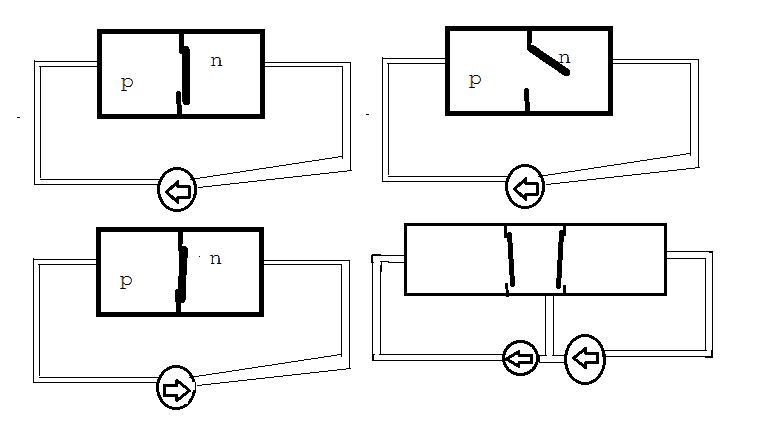
attachment.php?attachmentid=48232&stc=1&d=1339409662.png


Where has my analogy gone wrong?? What actually causes the fluid (current) flow at a higher rate through the second valve (Collector-base jucntion)??

Thanks in advance
 

Attachments

  • transistor.png
    transistor.png
    2.8 KB · Views: 598
Last edited:
Engineering news on Phys.org
  • #2
These things used to be all the rage:
http://blog.modernmechanix.com/fluid-transistor-circuits/ ... Modern Mechanics June 1960 :)
BTW: You cannot link to an image on your C: drive unless you run a file server. Better upload it someplace.
 
  • #3


the collector-base junction is reversed biased in a normal common-emitter circuit and that's the point! that's how current is controlled which (with a large Vc) get's you a current-controlled current source.

for charge-carriers coming from the emitter (electrons in the NPN case), if the transistor [itex]\beta[/itex] is about 99, that means for every 100 electrons that cross the (forward-biased) emitter-base junction, only 1 of those electrons "recombines" with a hole in the base, and since the base is very thin, the other 99 electrons make it all the way to the other side of the base (the collector-base junction) and when they see that juicy, large, and positive Vcb, they just can't resist.

normally, with a junction, reverse-biasing will cause that junction to be devoid of charge carriers on both sides of the junction and thus, it cannot conduct electricity. but the emitter supplies that charge and, if the base is thin (which results in a high current gain [itex]\beta[/itex]) much of that charge supplies what is otherwise missing at the collector-base junction. this is why soldering two diodes, back-to-back, won't work as a transistor.
 
  • #4


rbj said:
the collector-base junction is reversed biased in a normal common-emitter circuit and that's the point! that's how current is controlled which (with a large Vc) get's you a current-controlled current source.

for charge-carriers coming from the emitter (electrons in the NPN case), if the transistor [itex]\beta[/itex] is about 99, that means for every 100 electrons that cross the (forward-biased) emitter-base junction, only 1 of those electrons "recombines" with a hole in the base, and since the base is very thin, the other 99 electrons make it all the way to the other side of the base (the collector-base junction) and when they see that juicy, large, and positive Vcb, they just can't resist.

normally, with a junction, reverse-biasing will cause that junction to be devoid of charge carriers on both sides of the junction and thus, it cannot conduct electricity. but the emitter supplies that charge and, if the base is thin (which results in a high current gain [itex]\beta[/itex]) much of that charge supplies what is otherwise missing at the collector-base junction. this is why soldering two diodes, back-to-back, won't work as a transistor.

Actually if the beta is 99, the number of electrons emitted from the emitter that recombine in the base is more like 1 in 5,000. Base current is chiefly consisting of hole current from the base towards the emitter. Nearly all base current is this injection component. The transport component is the fraction of emitted electrons that recombine in the base, not surviving the trip to the collector. Just thought this should be mentioned.

Claude
 
  • #5


rbj said:
that means for every 100 electrons that cross the (forward-biased) emitter-base junction, only 1 of those electrons "recombines" with a hole in the base, and since the base is very thin, the other 99 electrons make it all the way to the other side of the base (the collector-base junction) and when they see that juicy, large, and positive Vcb, they just can't resist.


This is where I have a problem in understanding.. How can 99 electrons make it all the way to the other side? Shouldn't they be resisted by the reverse biased voltage? And how do we get large positive Vcb??
 
  • #6
PrakashPhy said:
This is where I have a problem in understanding.. How can 99 electrons make it all the way to the other side? Shouldn't they be resisted by the reverse biased voltage? And how do we get large positive Vcb??

Try this link.

http://www.allaboutcircuits.com/worksheets/bjt0.html

Study questions 6 & 13.
 
  • #7


PrakashPhy said:
This is where I have a problem in understanding.. How can 99 electrons make it all the way to the other side? Shouldn't they be resisted by the reverse biased voltage? And how do we get large positive Vcb??
Actually, the bias on the b-c junction attracts electrons. Draw it and you'll see for yourself.

Claude
 
  • #8


cabraham said:
Actually if the beta is 99, the number of electrons emitted from the emitter that recombine in the base is more like 1 in 5,000. Base current is chiefly consisting of hole current from the base towards the emitter. Nearly all base current is this injection component. The transport component is the fraction of emitted electrons that recombine in the base, not surviving the trip to the collector. Just thought this should be mentioned.

thanks, Claude. what i remember from my solid-state physics class 35 years ago is spotty. i forgot that there were both holes and electrons were moving in the base.

so with your numbers, 1 out of 5000 electrons recombine in the base and 4999 present themselves to the c-b junction. and for every electron that recombines there is 49 holes that move to the b-e junction (and get recombined in the emitter)?
 
  • #9


PrakashPhy said:
This is where I have a problem in understanding.. How can 99 electrons make it all the way to the other side? Shouldn't they be resisted by the reverse biased voltage?

no, they are attracted to the collector by that voltage.

And how do we get large positive Vcb??

by hooking it up to a power supply. like in the run-of-the-mill common emitter circuit.
 
  • #10


rbj said:
thanks, Claude. what i remember from my solid-state physics class 35 years ago is spotty. i forgot that there were both holes and electrons were moving in the base.

so with your numbers, 1 out of 5000 electrons recombine in the base and 4999 present themselves to the c-b junction. and for every electron that recombines there is 49 holes that move to the b-e junction (and get recombined in the emitter)?

You're thinking the right way. In addition, as frequency increases, the displacement current needed to charge/discharge the b-e diffusion capacitance increases. Thus beta drops off at the rate of a factor of 10 per decade of frequency. At the frequency labeled as "ft", the beta value is unity. This is the "transition frequency". BR.

Claude
 
  • #11


cabraham said:
... as frequency increases, the displacement current needed to charge/discharge the b-e diffusion capacitance increases. Thus beta drops off at the rate of a factor of 10 per decade of frequency. At the frequency labeled as "ft", the beta value is unity. This is the "transition frequency".

or the gain-bandwidth product?
 

1. How does conduction occur in reverse biasing?

Conduction in reverse biasing occurs when a voltage is applied in the opposite direction of the normal flow of current. This creates a depletion region in the semiconductor material, which allows for a small amount of current to flow through due to minority charge carriers.

2. Does conduction in reverse biasing have any practical applications?

Yes, conduction in reverse biasing is commonly used in devices such as diodes and transistors. It allows for the control of current flow and can be used in rectification and switching circuits.

3. How does conduction in reverse biasing differ from conduction in forward biasing?

In forward biasing, the voltage is applied in the same direction as the normal flow of current, allowing for a larger amount of current to flow through the material. In reverse biasing, the voltage is applied in the opposite direction, causing a smaller amount of current to flow due to the depletion region.

4. Is conduction in reverse biasing a reversible process?

Yes, conduction in reverse biasing is a reversible process. When the reverse bias voltage is removed, the depletion region disappears and the material returns to its normal conductivity.

5. How does conduction in reverse biasing affect the functioning of a transistor?

In a transistor, conduction in reverse biasing can be used to control the flow of current between the collector and emitter. By applying a reverse bias voltage to the base, the transistor can be switched off, while a forward bias voltage will turn it on.

Similar threads

Replies
5
Views
2K
  • Electrical Engineering
Replies
3
Views
795
Replies
3
Views
1K
Replies
42
Views
2K
  • Electrical Engineering
Replies
10
Views
2K
Replies
10
Views
1K
Replies
68
Views
4K
  • Electrical Engineering
Replies
5
Views
3K
Replies
16
Views
4K
Replies
19
Views
5K
Back
Top