Coupled inductor boost converter - Ripple current

AI Thread Summary
The discussion revolves around calculating ripple currents ∆i1 and ∆i2 in a coupled inductor boost converter, particularly during specific time intervals. The original poster is seeking assistance in deriving formulas for these ripple currents, expressing uncertainty about their correctness. Participants request additional details, such as schematics and waveforms, to provide better guidance. The conversation also touches on the unique topology of the converter and its advantages, especially in achieving higher boost ratios compared to conventional designs. Overall, the focus remains on deriving accurate expressions for ripple currents in the context of the boost converter's operation.
member 638480
I am trying to calculate the ripple current in boost converter for ∆i1 and ∆i2 between time intervals between DT and T, and also dependent on the voltage level (Vin or Vin-Vout). To find a formula for ∆i1 and ∆i2, two formulas have to be derived for them. This is done from the equation:
upload_2018-1-5_13-47-0.png

I derived equations for ∆i1 and ∆i2 as shown below, however I don't think this is right and I was wondering has anybody done this before that can provide some assistance, thanks!
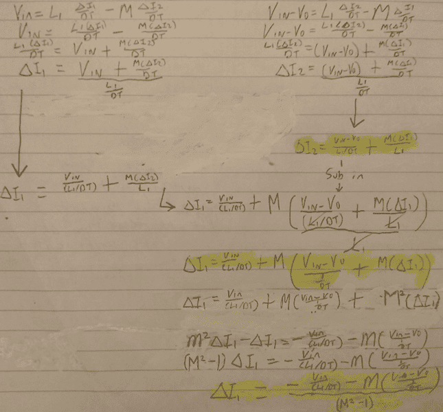
upload_2018-1-5_13-48-14.png
 

Attachments

  • upload_2018-1-5_13-41-20.png
    upload_2018-1-5_13-41-20.png
    83 KB · Views: 746
  • upload_2018-1-5_13-47-0.png
    upload_2018-1-5_13-47-0.png
    5 KB · Views: 1,203
  • upload_2018-1-5_13-48-14.png
    upload_2018-1-5_13-48-14.png
    87.8 KB · Views: 1,330
Engineering news on Phys.org
Tommy Drudy said:
I am trying to calculate the ripple current in boost converter for ∆i1 and ∆i2 between time intervals between DT and T, and also dependent on the voltage level (Vin or Vin-Vout). To find a formula for ∆i1 and ∆i2, two formulas have to be derived for them. This is done from the equation: View attachment 217893
I derived equations for ∆i1 and ∆i2 as shown below, however I don't think this is right and I was wondering has anybody done this before that can provide some assistance, thanks!
View attachment 217894
Welcome to the PF. :smile:

Can you post your schematic and time-domain waveforms with all of the times and such listed? Thanks, we should be able to help you on this.

BTW, is this for schoolwork?
 
Below is a screenshot of VL1 and VL2, it shows the voltage and ripple current when the switch is either on or off due to interleaving. The only unknown variables from the formula mentioned in my previous post is ∆i1 and ∆i2, which is replicated by the red line in this photo. That is why I am trying to derive an expression for the two ripple currents, in order to find their value at each point, ie DT, T/2, DT+T/2, and T.
upload_2018-1-5_17-21-55.png

This question is for a boost converter that I am trying to design as part of an assignment.
 

Attachments

  • upload_2018-1-5_17-9-3.png
    upload_2018-1-5_17-9-3.png
    16.5 KB · Views: 716
  • upload_2018-1-5_17-9-43.png
    upload_2018-1-5_17-9-43.png
    15.4 KB · Views: 765
  • upload_2018-1-5_17-21-55.png
    upload_2018-1-5_17-21-55.png
    37.7 KB · Views: 1,149
juniorbvetran said:
Below is a screenshot of VL1 and VL2, it shows the voltage and ripple current when the switch is either on or off due to interleaving. The only unknown variables from the formula mentioned in my previous post is ∆i1 and ∆i2, which is replicated by the red line in this photo. That is why I am trying to derive an expression for the two ripple currents, in order to find their value at each point, ie DT, T/2, DT+T/2, and T.
View attachment 217902
This question is for a boost converter that I am trying to design as part of an assignment.
You didn't attach the schematic yet. Is this a flyback topology Boost converter?
 
berkeman said:
You didn't attach the schematic yet. Is this a flyback topology Boost converter?
Apologies, the topology is below, no its not a flyback.
upload_2018-1-5_17-32-10-png.png
 

Attachments

  • upload_2018-1-5_17-32-10-png.png
    upload_2018-1-5_17-32-10-png.png
    7.9 KB · Views: 730
Interesting! I hadn't seen that topology before, but I work with Buck converters a lot more than Boost converters. Can you say more about it? Where did you find it? I can see the motivation for using 2 inductors, but why use coupled inductors? Thanks.
 
berkeman said:
I did a little Google searching on your thread title, but this topology is different than what you have posted so far...

http://www.onsemi.com/pub/Collateral/AN-5081.pdf.pdf
Ya I am not to sure, i just know the equations are used to derive the ripple current. I've had a good look around for a final derivation of the ripple current formula but there doesn't seem to be anything online.
 
I'm not intuitively seeing how the coupled inductor part would help the ripple current. Have you seen anything about the coupled inductor part of it?

If not, I'm sure others can chime in who have seen this topology before. Or worst case I can run a simulation on it this weekend at work (in all of my spare time... Ack). :smile:
 
  • #10
berkeman said:
I did a little Google searching on your thread title, but this topology is different than what you have posted so far...

http://www.onsemi.com/pub/Collateral/AN-5081.pdf.pdf
It looks like that (different) boost topology with coupled inductors is to get a higher boost ratio:
Conventional step up dc-dc converters or boost converters
are not suitable for high voltage conversion ratio since the
effective series resistor (ESR) of the boost inductor
prohibits the output voltage from increasing more than 10
times of the input voltage.In this article, a high step-up dc-dc converter
with tapped inductor or coupled inductor is introduced and its
operational principle and design procedure will be described
as well.

Where did you get your circuit from?
 
Last edited:

Similar threads

Replies
13
Views
3K
Replies
8
Views
3K
Replies
14
Views
2K
Replies
8
Views
2K
Replies
3
Views
4K
Replies
9
Views
4K
Replies
3
Views
2K
Replies
17
Views
3K
Back
Top