mariost
- 5
- 0
A Tesla coil is an electrical resonant transformer circuit designed by inventor Nikola Tesla in 1891. It is used to produce high-voltage, low-current high frequency alternating-current electricity.
Tesla tried to transfer energy with a wireless way. It was really difficult to do this to a long distance and as you had to increase the current for this , the experiment was dangerous . So the project stopped.
Today, their main use is for entertainment and educational displays.
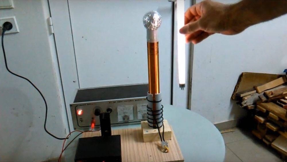
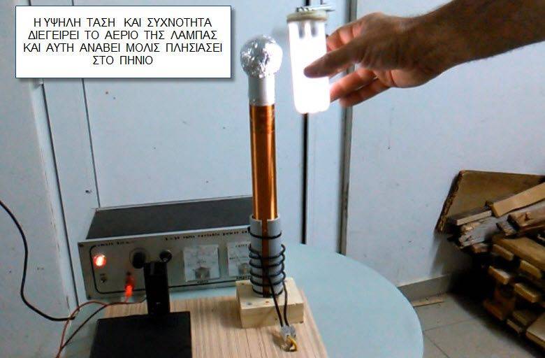
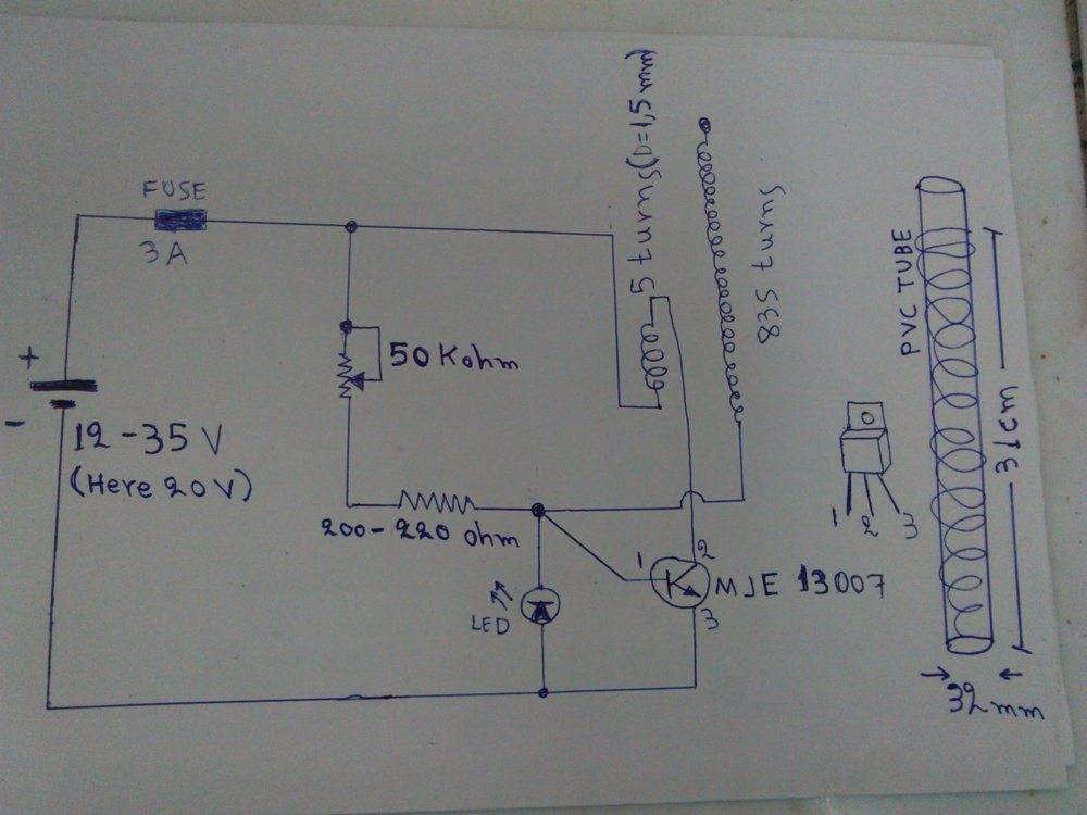
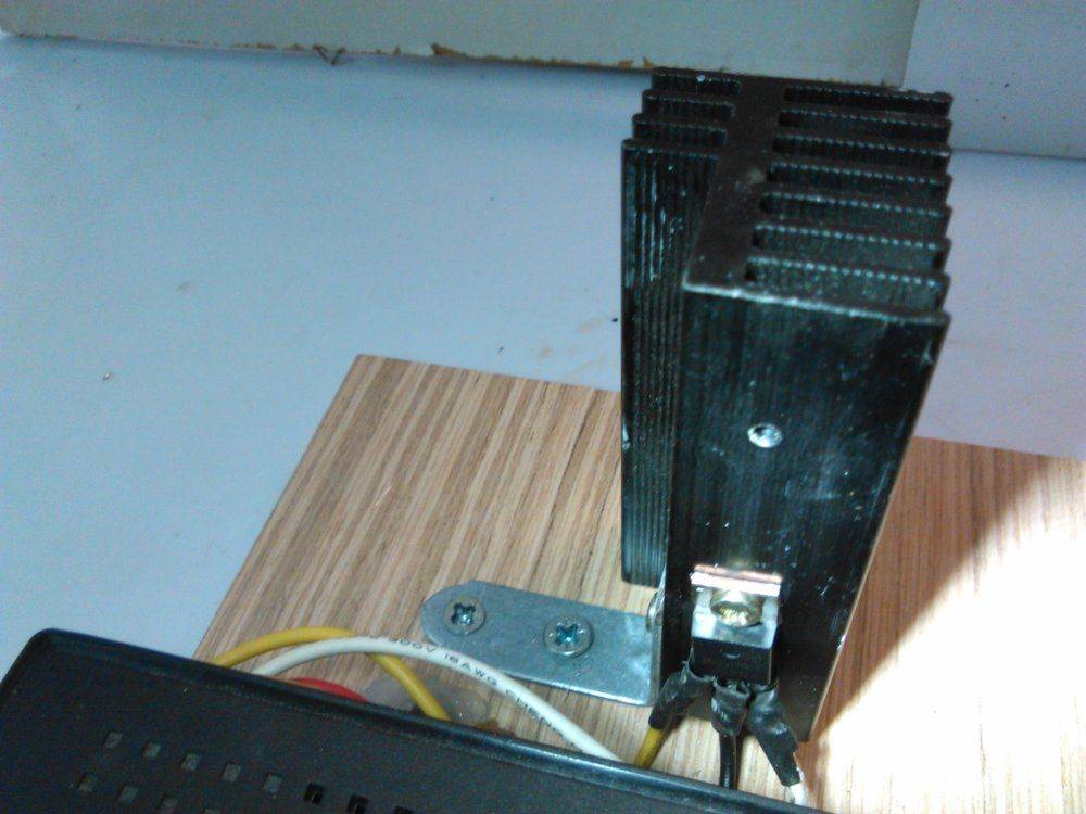
In my Tesla coil I used a circuit with a MJE 13007 transistor that cuts and connects the current to the primary coil very quickly and produces a high voltage current with big frequency to the secondary coil. This is the reason that makes the ionization of the gas to this kind of bulbs.
I used a 1.5 mm diameter wire with 5 turns to the primary coil and a 0.3 mm with 830 turns to the secondary.
The experiment is not dangerous. The current is very low in the secondary and this kind of current ( very big voltage –very big frequency – very low current) passes through the surface of the skin.You can smell the skin that burns if you touch the antenna for 3-4 second or more. Nothing else. If you want to see bigger spark you must use more powerful power supply. About 30-40 volts and more than 100 w. YOU CAN WATCH THE CONSTRUCTION AND THE USE HERE:
Last edited by a moderator: