Engineering Construct a circuit diagram of a step-up chopper in Multisim

  • Thread starter Thread starter Fatima Hasan
  • Start date Start date
  • Tags Tags
    Circuit Diagram
AI Thread Summary
The discussion focuses on troubleshooting a step-up chopper circuit simulation in Multisim, where the output voltage remains constant despite varying resistance. Participants emphasize the importance of ensuring that the switching transistor (Q1) is properly driven by the 555 timer IC, as a lack of drive results in no boost action. They discuss expected waveforms for the inductor and diode currents, noting that the inductor current should exhibit a triangular shape due to its charging and discharging behavior. Additionally, suggestions include reviewing the 555 timer datasheet for proper connections and considering the impact of circuit parameters like inductance on performance. The conversation highlights the need for careful analysis of circuit behavior to achieve the desired voltage output.
Fatima Hasan
Messages
315
Reaction score
14
Homework Statement
Attached below.
Relevant Equations
-
Using any Electrical Engineering software:
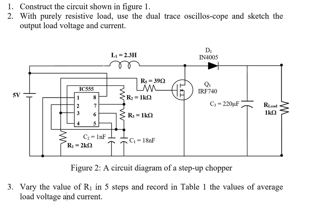
screenshot-115.png

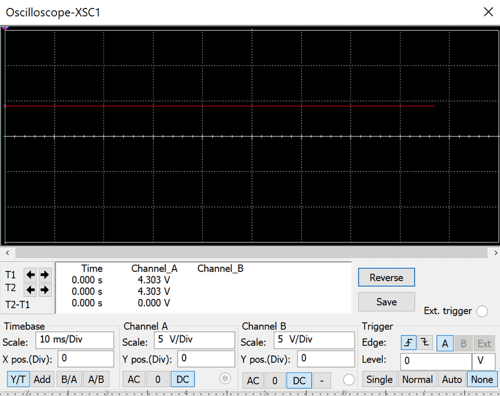
I tried to simulate using Multisim, but the output voltage remains constant even after varying R1. Also, I only got the voltage from the oscilloscope, but how to find the current ?
Here's my attempt:
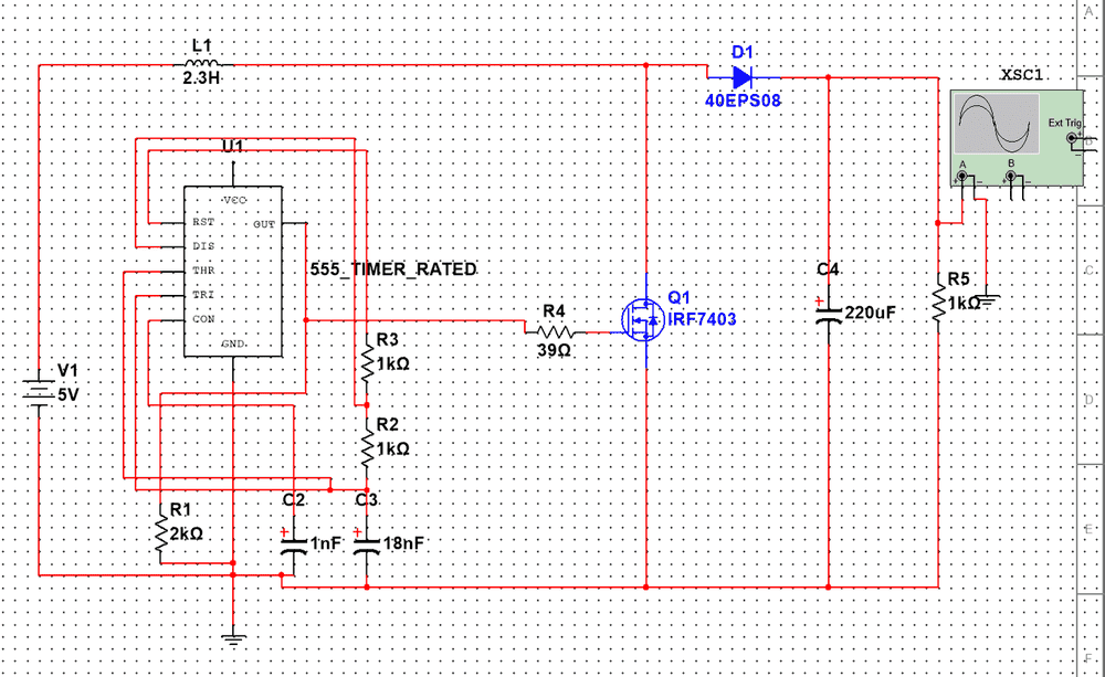
screenshot-127.png

screenshot-115.png


Any help would be greatly appreciated!
 
Last edited:
Physics news on Phys.org
How can you use the clue that the output voltage is one diode drop below the input 5V? :smile:
 
berkeman said:
How can you use the clue that the output voltage is one diode drop below the input 5V? :smile:
Sorry, I didn't understand what you mean.
 
Fatima Hasan said:
Sorry, I didn't understand what you mean.
Well, when I looked at your simulation, I expected to see an output voltage that is higher than the input 5V source. That's what the "Boost" chopping action of Q1 does in that circuit when it is running correctly. There's pretty much only one main way that the output voltage could be one diode drop below the input 5V supply in a Boost circuit. Have you put a 'scope probe on the drive for Q1 and on Q1's drain? What do those test points show?
 
berkeman said:
Well, when I looked at your simulation, I expected to see an output voltage that is higher than the input 5V source. That's what the "Boost" chopping action of Q1 does in that circuit when it is running correctly. There's pretty much only one main way that the output voltage could be one diode drop below the input 5V supply in a Boost circuit. Have you put a 'scope probe on the drive for Q1 and on Q1's drain? What do those test points show?
screenshot-128.png
/

That's what I got :
screenshot-129.png
 
Looks flatline in the window in time that you are looking at the drive. You need to be sure that your Q1 is being driven by the 555 IC. If there is no drive, there is no Boost...
 
I'm not seeing any power connection to the 555. Also, don't you have to connect the ground on your scope channels?
 
DaveE said:
I'm not seeing any power connection to the 555. Also, don't you have to connect the ground on your scope channels?
screenshot-130.png

Xsc1 :
screenshot-131.png


After connecting the other channels to ground on scope 1:

screenshot-132.png
 
berkeman said:
Looks flatline in the window in time that you are looking at the drive. You need to be sure that your Q1 is being driven by the 555 IC. If there is no drive, there is no Boost...
Q1 is connected to R4 which is connected to the IC555.
 
  • #12
Fatima Hasan said:
I think they should be triangular waveforms , right ?
Which "they" waveforms? Not the gate drive voltage...

The overall inductor current does have a triangular shape (why?), but the diode and transistor switch currents are not exactly regular triangle waves (why not?).

https://en.wikipedia.org/wiki/Boost_converter

1588713625933.png
 
  • #13
berkeman said:
The overall inductor current does have a triangular shape (why?),
In the ON-state,diode is off : the current flows through the inductor ( charging) and the inductor stores the energy.
In the OFF-state, (Discharging),diode is ON: the inductor will act as a source and the diode makes the inductor to flow a current from itself and the energy will be dissipated. Since the switch cycled fast , the current won't reach 0 .
 
Last edited:
  • #14
berkeman said:
How can you use the clue that the output voltage is one diode drop below the input 5V? :smile:
try this
رافع جهد.JPG
 
  • #15
I suggest that you look at the data sheet for the 555 timer, especially the circuit for Astable operation. Then compare your connections on the 555 to what is in the data sheet.

The datasheet for the LM555 by Texas Instruments is quite informative.

Cheers,
Tom

p.s. Please keep us updated on your progress.
 
  • #16
Tom.G said:
I suggest that you look at the data sheet for the 555 timer, especially the circuit for Astable operation. Then compare your connections on the 555 to what is in the data sheet.

The datasheet for the LM555 by Texas Instruments is quite informative.

Cheers,
Tom

p.s. Please keep us updated on your progress.
Hello Mr. Tom,
Could you please check attached circuit and I would like to ask if I can step up voltage more and connect it to mobile power bank as volt source (as shown the current 17.3A )
Overloading may damage the battery!
Thanks

1684578549474.png
 
  • #17
The problem here is the high Q and low resonant frequency of the series LC tank circuit with 2.3 Henries and requires at least 5 or more cycles to settle. With 2.3H changing to 2.3uH is best.

Then it is becoming lower reactance, over damped but faster response.

Compute timescale / div to 1 cycle at resonant frequency. T= 2pi sqrt(LC)


Although settling time , damping factor changes with duty cycle as switch blocks inductive series impedance.

- reducing L by 6 orders of magnitude to uH also raises the output voltage ratio by only about 6 times not 6 million. due to load regulation and impedance ratios.
 
Last edited:
Back
Top