Reverse-Flow Protection Mosfet Control?

  • Thread starter M de L
  • Start date
  • Tags
    Mosfet
In summary, "Reverse-Flow Protection Mosfet Control" refers to a method of preventing reverse current flow in electronic circuits using MOSFETs (Metal-Oxide-Semiconductor Field-Effect Transistors). This control mechanism ensures that current can only flow in the intended direction, thereby protecting sensitive components from damage caused by unintended reverse currents. The implementation typically involves the use of a control circuit that monitors voltage levels and activates the MOSFET to block reverse flow when necessary, enhancing the reliability and efficiency of electronic systems.
  • #1
M de L
7
1
TL;DR Summary
Can anyone please explain how this circuit's reverse-flow protection Mosfet is turned on and off?
Hi,

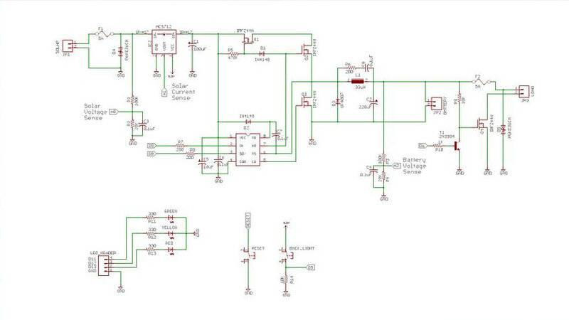
Attached is a circuit diagram for a solar powered, synchronous Buck converter. It appears to have and extra Mosfet, Q1, that is intended to prevent the flow of current, out from the battery, and back toward the unlit solar panel, via the body diode of Q2. Q2, being the regulator's high-side Mosfet.

I'm okay with how the synchronous Buck converter works, including the bootstrap drive from the Mosfet driver chip. What I don't get, is how Q1 is turned on and off, from the high-side Mosfet's gate drive signal.

Can anyone please explain this to me? Is this a conventional, and reliable configuration?

M.
FL22QOII6EXG10K.jpg
 
Engineering news on Phys.org
  • #2
M de L said:
What I don't get, is how Q1 is turned on and off, from the high-side Mosfet's gate drive signal.
Can anyone please explain this to me? Is this a conventional, and reliable configuration?
The picture is a bit blurry, but I believe the designer of that circuit knew exactly what they were doing. The clue is in an N-channel device, weirdly, (though not irrationally), connected to the positive supply input.

Q1 appears to be there to protect the circuit from a reversed polarity supply, in effect, an efficient "idiot diode". The gate resistor can be a few kΩ, as it does not need to change the gate voltage of Q1 rapidly.

If polarity is OK, the Q1 (normally reversed) body-diode will turn on, then the MOSFET will begin to conduct due to the gate signal, effectively shorting the body-diode to reduce Q1 device power and voltage drop.

If polarity is reversed, Q1 will operate normally, by turning off. The body-diode will be reverse biased, as expected. The circuit is then protected from the reversed input connection.

It may at first seem counterintuitive, but that is a "more than reliable" connection of a MOSFET, that protects the following circuit from reversal of the input connections.
 
  • Like
Likes M de L and Nik_2213
  • #3
Ah, Thank you, Baluncore. Q1's value as a reverse polarity protection hadn't occurred to me. Okay, how it turns off during reverse polarity connection seems to make sense. Very clever.

How Q1 then turns on, depending on the gate signal through D1 is a mystery? I get that Q1 can conduct current from source to drain when turned on (opposite to how it's usually used), but how we arrive at a sufficiently positive voltage, from the gate to the source, to turn Q1 on, defies my understanding?

Suppose the high-side Mosfet gate drive signal is low, relative to the half bridge's switched pole. Is it true that current cannot then flow backwards from the battery, to a non-illuminated solar panel? It would just be very convenient if the reverse polarity protecting isolator, Q1, could double as an isolator to prevent any reverse current flow, through the high-side Mosfet's body diode as well?
 
  • #4
If possible I'd like to see a clearer image. Thank you.
 
  • #6
Okay, seems the part of the circuit of interest, doesn't actually work. From the Instructables article:

"The other problem was that MOSFET Q1 ( in V-3.0) conduct even when there is no solar input."

Identical 'protective' mechanisms appears in a number of similar solar charger projects, so maybe it's been propagated.

Yet other projects leverage an anti-reverse current flow control Mosfet, gate-driven by an isolated DC supply that can be switched. Maybe that's the way to go, and there are no easy shortcuts?
 
  • #7
Yes, a better schematic would be nice. It looks to me like this one has Q1 drawn incorrectly. It looks like it's drawn as a P-Channel MOSFET, But I agree with @Baluncore's description since the source is on the wrong side. So, anyway, we'll just chalk this up to poor documentation, which is common on DIY style web sites.

As an aside, this is a good description of "normal" reverse polarity protection schemes. It all seems sort of confused in this example. Just pick a version yourself a stick it in place of that stuff.

So, the answer to your question "how does Q1 get the bias voltage needed to turn on?" is that the half-bridge gate drive IC provides this with a bootstrap circuit. This is a capacitor charge pump like a voltage multiplier. This is also needed to turn on the high side MOSFET (Q2?). Read the data sheet for the IC, it should explain it.
 
  • #8
M de L said:
there are no easy shortcuts?
If you mean that you have to understand each part of your circuit, then, yes, I agree. If you mean reverse polarity protection isn't easy, then I think your wrong. You can figure it out.
 
  • #9
I question the functionality of Q2 specifically. Doesn't the gate-source voltage need to be several volts apart before the mosfet turns on hard? The way it is, the gate can go no higher than the drain unless I've missed something. This implies the source will never make it all the way to the drain voltage meaning heat dissipation in Q2. Have I missed something here?
 
  • #11
Thanks @DaveE. I was wondering about the D2-C7 pair formed a voltage doubler but I expected a larger capacitor. Guess the .1 uF is adequate. As well as the little 1N4148 diode.
 
  • Like
Likes DaveE

FAQ: Reverse-Flow Protection Mosfet Control?

What is Reverse-Flow Protection in MOSFETs?

Reverse-flow protection in MOSFETs refers to the mechanism that prevents current from flowing in the reverse direction through the MOSFET when it is turned off. This is crucial in circuits where backflow could damage components or lead to inefficient operation. Typically, this is achieved using a combination of MOSFETs and control circuitry to ensure that the device remains off during undesired conditions.

How does MOSFET control work for reverse-flow protection?

MOSFET control for reverse-flow protection works by utilizing a control signal to turn the MOSFET on or off based on the current direction and voltage levels. When the forward current is detected, the MOSFET is turned on, allowing current to flow. If the current attempts to reverse, the control circuitry detects this condition and turns the MOSFET off, thereby preventing reverse current flow.

What are the advantages of using MOSFETs for reverse-flow protection?

The advantages of using MOSFETs for reverse-flow protection include low on-resistance, which reduces power loss, fast switching speeds that enhance circuit efficiency, and the ability to handle high currents. Additionally, MOSFETs can be easily integrated into various circuit designs, providing flexibility in applications such as power supplies and battery management systems.

What are common applications of reverse-flow protection MOSFET control?

Common applications of reverse-flow protection MOSFET control include power supply circuits, battery charging systems, solar inverter designs, and motor driver circuits. In these applications, preventing reverse current flow is critical for maintaining system integrity and ensuring safe operation.

What are the limitations of reverse-flow protection using MOSFETs?

Limitations of reverse-flow protection using MOSFETs include the need for additional control circuitry, which can increase complexity and cost. Additionally, the performance can be affected by temperature variations and the characteristics of the MOSFET itself, such as threshold voltage and switching speeds. Furthermore, if not designed properly, there can be a risk of voltage spikes that may damage the MOSFET.

Back
Top