Weaver
- 70
- 6
- Homework Statement
- As part of a VLSI lab, we're designing an Operational Transconductance Amplifier chip. I'm struggling with understanding the OTA circuit. As part of design verification, we're supposed to build a voltage follower circuit and run simulations. With this, there is two things I don't quite follow:
1.How to decide the biasing condition?
2.Which feature of the OTA will decide the compatibility of the load?
- Relevant Equations
- Iout =g(V+- V-)
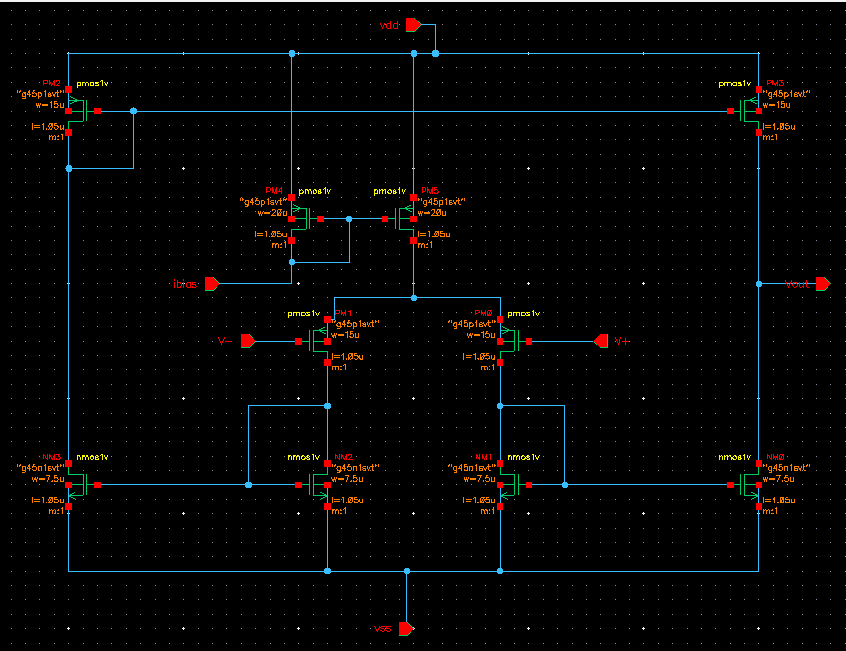
My attempt at the OTA is as follows:
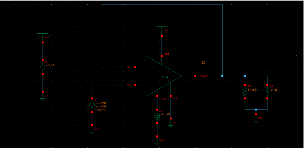
The simulation circuit is as follows:
I've gotten this far largely due the nature of the handout and its hints. I'm struggling with understanding ibias
From my understanding, there is a current mirror at the top of the OTA. This creates an infinite input impedance, matching the op amp design. From there I guess ibias has to be high enough to force PM5 into saturation? But I'm not sure how to find this value?
From experimenting with the simulation, it has to be in the range 1nA to 10mA, but I have no real idea why...
As for the load compatibility, my understanding of the OTA is, it produces a current proportional to the voltage difference at the inputs. So to make the circuit a voltage follower, you have to convert this current to a voltage? And the RC circuit does this by charging the capacitor? So the output current would decide the compatibly of the load? Or is it to do with the high output impedance of the OTA?
Any help or guidance would be really appreciated. Thank you!
The simulation circuit is as follows:
I've gotten this far largely due the nature of the handout and its hints. I'm struggling with understanding ibias
From my understanding, there is a current mirror at the top of the OTA. This creates an infinite input impedance, matching the op amp design. From there I guess ibias has to be high enough to force PM5 into saturation? But I'm not sure how to find this value?
From experimenting with the simulation, it has to be in the range 1nA to 10mA, but I have no real idea why...
As for the load compatibility, my understanding of the OTA is, it produces a current proportional to the voltage difference at the inputs. So to make the circuit a voltage follower, you have to convert this current to a voltage? And the RC circuit does this by charging the capacitor? So the output current would decide the compatibly of the load? Or is it to do with the high output impedance of the OTA?
Any help or guidance would be really appreciated. Thank you!