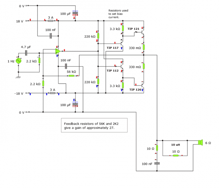
Analyse this amplifier for me please :)

In summary, this amplifier uses an Ne5532p op-amp for the voltage amplification and feedback in the non-inverting configuration. The output stage is handled by two Darlington transistors, TIP 121 and TIP 126. These are hopefully biased by TIP 117 and TIP 112. The amplifier can output up to 25w into 4Ω@ ±18v.
  • #1
Gingerbunny82
13
0
Hi folks, I've designed this amplifier, it uses an Ne5532p op-amp for the voltage amplification and feedback in the non-inverting configuration. The output stage is handled by two Darlington transistors, TIP 121 and TIP 126, these are hopefully biased by TIP 117 and TIP 112.

I was hoping that some more experienced engineers could take a look at this circuit and give me feedback on its performance, and any tips to improve it would be greatly appreciated.

I have managed to build this circuit and it sounds okay to me, I can't hear any distortion, even at low volumes, but are my ears deceiving me? It operates off +- 18v, and I was also wondering about the output stage, is it operating in class AB, or is it purely a class B stage? I don't think it's class B because surely the crossover distortion would be horrible but If you guys could clear up my confusion I would greatly appreciate it, many thanks,
snipd.PNG
 
Engineering news on Phys.org
  • #2
Gingerbunny82 said:
are my ears deceiving me?
The way to find out would be to take a digital sample of the input and output, then do some kind of statistical analysis of the comparison instead of using your ears.
 
  • Like
Likes Gingerbunny82
  • #3
assuming you did all the math on the biasing right you'll need a scope to check the transistor inputs as well as running a function generator with sine wave and doing a sweep, one thing I do notice that your missing is a low pf cap across the 56k resistor to prevent high frequency oscillation.
 
  • Like
Likes Gingerbunny82
  • #4
on second thought I notice another problem, your output bias, you don't have any positive feedback for the output transistors thermal regulation and you may have a problem with the input and/or output transistors where you'll need .7 volts lifted at the gates, this can be done with a couple of small signal diodes in the right place.

/me waits for a more experienced member to comment.
 
  • Like
Likes Gingerbunny82
  • #5
What output power do you want from this amplifier ??
Well I see you try to use a diamond buffer as a output stage. But why with two Darlingtons ?
Also your output stage quiescent current is not well defined. Because now your quiescent current depends on vbe mismatch.
Also connect your power supply directly to output stage and use RC for supply the OpAmp.
 
  • Like
Likes Jeff Rosenbury and Gingerbunny82
  • #6
If you download a copy of the free LTspice from the Linear Technology site you will be able to simulate it yourself.
http://www.linear.com/designtools/software/
If you have problems getting LTspice or your circuit to work you can ask or attach .asc files as text files to a PF post.
 
  • Like
Likes Gingerbunny82
  • #7
Firstly, many thanks for the replies folks,
you may have a problem with the input and/or output transistors where you'll need .7 volts lifted at the gates,
- I was under the impression that this voltage was provided by the driver transistors TIP 117 and TIP 112, is this incorrect?

What output power do you want from this amplifier ??
- I was hoping to get around 25w into 4Ω @ ±18v. Is this obtainable, my circuit draws 30mA with no input connected.

But why with two Darlingtons ?
- I ordered them by accident, so I tried to make them work I realize its not ideal. The downside is my circuit seems to clip @ ±14.5v with power rails @ ±18v. I think this might be because the darlingtons require around 1.2v to turn on, is this correct? Or could it be the op-amp not capable of reaching the rails.

Also your output stage quiescent current is not well defined. Because now your quiescent current depends on vbe mismatch.

- Should I make the TIP 117 and TIP 126 drivers say both TIP 126 instead so they are the same part. Then do the same with the NPN transistors.
Leaving me with matching pairs? Would this help?

Many thanks :)
 
  • #8
How can you make both outputs the same part when one needs to be PNP and the other NPN? I would say you are correct in saying that the way the driver transistors are configured should bias the outputs correctly. However, this assumes the drivers base-emitter voltage is similar to the outputs base-emitter voltage. If the outputs are darlingtons then of course this won't be true.
 
  • #9
Thanks for your input Averagesupernova,

How can you make both outputs the same part when one needs to be PNP and the other NPN?

What I meant is make all the NPN transistors the same model and all PNP transistors the same, so the above schematic would have (2x) TIP 121 NPN and (2x) TIP 126 PNP.
 
  • #10
http://www.douglas-self.com/ampins/books/apad.htm

I have all his books, I consider him a god when it comes to amplifier design, I highly suggest you get this book.

here is some more reading: http://www.allaboutcircuits.com/textbook/semiconductors/chpt-4/cascode-amplifier/

and if you want to show off your amp check out diyaudio.com tons of useful info there.
 
Last edited:
  • Like
Likes Gingerbunny82
  • #11
I would not make the drivers the same as the outputs. The base currents will be much larger in the outputs compared to the drivers so the base-emitter voltage drop will also be different and you want the to be as close to the same as possible.
 
  • Like
Likes berkeman
  • #12
I've not used a diamond buffer.

It looks like it would have a low output impedance, but the input impedance seems high due to the ß > 1000 of the darlingtons. Since your emitter resistors are in series with the load, the input resistance to the darlinton emitter follower stage will vary with your speaker impedance (which dominates the input resistance equation). The speaker impedance varies with frequency. This might cause an impedance mismatch between your biasing transistor stage and your darlington stage that will vary with frequency. It should be a small effect and act somewhat like a graphic equalizer, so it's no big deal unless you're an audiophile. (The mismatch seems to be varying from about the right value to several times too high. Too high is better than too low.)

Or I could be wrong.
 
  • #13
The negative feedback in this amplifier should help a lot with frequency response.
 
  • #15
I can see where this output stage cannot be expected to drive very close to power supply rails as the only thing pulling on the base of the output transistors is a resistor. A somewhat clever biasing scheme though. I had never seen this til now but it jumped out at me and made sense.
 
  • #16
So what sets the quiescent current at 0 volts out to make it class AB.
 
  • #17
meBigGuy said:
So what sets the quiescent current at 0 volts out to make it class AB.

The output stage is push-pull. Any quiescent current flowing through the speaker will cause a small voltage drop which will feed back to the negative input of the op-amp, changing the bias points of the push-pull transistors to limit the current. It's a small effect, but it only needs to overcome the mismatch in the darlinton betas.

The quiescent bias current through the darlingtons seems a little wonky since they are being biased by the voltage drop across a regular BJT. (They "should" have twice that.) I think that would limit their RF response, but I don't think it matters much at audio frequencies. It does mean a low quiescent current through the darlingtons, but I don't see a problem there; more of a feature really. (There's a lot of non-linearity as well, but with a push-pull pair I don't think that's a problem either.)

A very clever design.
 
  • #18
The circuit is not bad, but there are some areas that could stand an analysis and a redesign. Off the top of my head:
  • The power dissipation in the driver transistors will be a bit on the high side
  • Since there is almost no local feedback, only an overall feedback, I see a possible problem with TIM (Transient Intermodulation Distortion)
I suggest that you take a look at http://www.w5dor.com/AppNotes/AN485-Hi-Power-Audio-Amps.pdf for a thorough discussion of the stages in a Hi-Fi amplifier.
 
Last edited by a moderator:
  • #19
Svein said:
The circuit is not bad, but there are some areas that could stand an analysis and a redesign. Off the top of my head:
  • The power dissipation in the driver transistors will be a bit on the high side
  • Since there is almost no local feedback, only an overall feedback, I see a possible problem with TIM (Transient Intermodulation Distortion)

Why will the power dissipation be high? The current and voltage drop need to be dissipated somewhere. Admittedly there are switched amplifiers with lower dissipation, but power transistors are built for this sort of job. Make sure the heat sink is up to the task. (He said he built the circuit around the darlingtons, so I assume they are expensive/hefty.)

It's my understanding TIM is when non-linear amplifiers unintentionally act as mixers. Push pull amps are tend to be pretty linear. That applies to the op-amp as well as the darlington stages. So the bias transistors would be the problem children. They look to be emitter followers with a linear gain ≅ their beta, but perhaps I'm missing something.
 
  • #20
Jeff Rosenbury said:
It's my understanding TIM is when non-linear amplifiers unintentionally act as mixers.
No. The Ottala paper states that TIM is due to clipping and saturation in the intermediate stages when little or no local feedback is used. See http://www.shabad.ru/IEEE/otala.pdf.
Jeff Rosenbury said:
Why will the power dissipation be high? The current and voltage drop need to be dissipated somewhere.
Yes, but in a power amplifier class AB the current in the output stages is kept low when the signal is small. The drivers in this case are constantly driving a current through the emitter resistor (about 6mA) with a voltage across them of about 18V (18V*6mA = 108mW). Again, see my reference for a very good design.
 
  • #21
I'm not sure I understood all that. It's been a while since control theory.

But what I think it's saying is that the maximum frequency is limited by something akin to the gain/bandwidth product. When higher frequency signals come in they drive the system to the rails which limits low frequency gain to 1 which is non-linear (at least for a small bit) and mixes. Darlingtons have lots of parasitic capacitance, so that amplifies the problem. But the voltage gain is only 28 (as opposed to 100 or more for typical applications) so that limits the problem. These transistors seem to be made for about 100 kHz operation. (It was hard to tell from the data sheet, but they used that value in a test.) It gives a collector-base capacitance (~150 pF at 18V) but I think the important value would be internal. (The collector-base capacitance on the first transistor inside the pair is important, I think.) Anyway, I have no idea how to figure what the cutoff frequency is. 100 kHZ is clearly problematic, but I'm sure the transistor can manage well above that. Just how far?...

I can see where limiting the high frequency end of the input could help eliminate this problem. Maybe toss in a filter set for 30 kHz or so.
 
  • Like
Likes Gingerbunny82
  • #22
I am not sure power dissipation in the driver stage is that big of a deal compared to other schemes. It's going to take so much drive on the bases of the outputs to get so much power out of them. After a certain point this probably requires an emitter follower (which is exactly what this design uses) and this often means some power dissipated in an emitter resistor. This brings up another point. Does an emitter follower technically have feedback built in with its emitter resistors? When we think of a common collector transistor stage we think of the emitter resistors being part of a feedback path. I would say that the point of the overall feedback in this circuit is to flatten the frequency response and keep the output at zero volts DC. The voltage gain from the output of the op-amp in the first stage to the speaker output is slightly less than one. Pretty hard to apply more 'local' feedback here. I think for what it is in components it is a nice little circuit. I don't think anyone should expect it to outperform the output circuits available in IC form. That would be silly.
 
  • Like
Likes Gingerbunny82
  • #23
In a class AB amplifier, current should flow through the output transistors when the output voltage is exactly zero. That is, a reliable quiescent bias current through the final PNP and the npn NPN when the speaker voltage is exactly zero. How is that accomplished here?
 
  • #24
Hi folks thank you for all your replies, I have been reading through them carefully. Svein I will take a look at that link, thank you. And thank you thankz (lol) for the book suggestion - looks good.

I have not changed the circuit yet, but I have taken some measurements @ ±18v of the circuit which I have here on the breadboard.
The new measurements are in pink.

These measurements are taken with NO input signal, and with a 6Ω speaker connected.

snipe.PNG
 
  • #25
meBigGuy said:
In a class AB amplifier, current should flow through the output transistors when the output voltage is exactly zero. That is, a reliable quiescent bias current through the final PNP and the npn NPN when the speaker voltage is exactly zero. How is that accomplished here?
The darlington pair is somewhat under-biased, but there is some bias voltage/current. Thus the quiescent current is near, but not at zero. In high frequency applications this would probably slow the response. But I doubt it's a problem in audio applications.
 
  • #26
Jeff Rosenbury said:
The darlington pair is somewhat under-biased, but there is some bias voltage/current. Thus the quiescent current is near, but not at zero. In high frequency applications this would probably slow the response. But I doubt it's a problem in audio applications.

- The TIP 126 data sheet says it has a small signal current gain Hfe of 1800 up to 20khz, the 3K3 resistor provides a base current of 5mA. If I make 3K3 a lower value say 1K5 the amplifier sounds horrible. Distorting even at low volumes. Why is this?
 
  • #27
meBigGuy I don't understand why you still have not been able to see how the outputs are biased up. The base voltage on the drivers is zero. Each one is it's own emitter follower all by itself. The voltages shown in post #24 make good sense. However, those outputs should not have been darlingtons and I don't think anyone here will argue that. As Jeff Rosenbury said they are somewhat underbiased. I suppose you could add diodes in the emitters of the drivers to take care of this.
 
  • #28
Gingerbunny82 said:
- The TIP 126 data sheet says it has a small signal current gain Hfe of 1800 up to 20khz, the 3K3 resistor provides a base current of 5mA. If I make 3K3 a lower value say 1K5 the amplifier sounds horrible. Distorting even at low volumes. Why is this?

I think you may be mis-analyzing the bias current to the darlingtons. (Or maybe I am?) Since the quiescent output of the op-amp is zero(ish), the biasing transistors will be operating at some normalish bias. That means they will drop (typically) 0.6 to 0.7 V (one diode drop). Since a darlington has two diode drops, it won't be fully biased. But if we recall our Eber Molls' model, even under-biased, there is some (small) current. That makes it operate in a non-linear mode, but since it's a push-pull, that shouldn't be a problem.

The rest of what you thought was the bias current will drain through the biasing transistors.

BTW, these are explanations are of what I think is happening. Your biasing obviously works. That makes it good.

I have don't know specifically why mis-biasing causes distortion. It may be that the op-amp is being overdriven by the current? (It will only source 10 mA, I think.)
 
  • #29
Jeff Rosenbury said:
I think you may be mis-analyzing the bias current to the darlingtons. (Or maybe I am?) Since the quiescent output of the op-amp is zero(ish), the biasing transistors will be operating at some normalish bias. That means they will drop (typically) 0.6 to 0.7 V (one diode drop). Since a darlington has two diode drops, it won't be fully biased. But if we recall our Eber Molls' model, even under-biased, there is some (small) current. That makes it operate in a non-linear mode, but since it's a push-pull, that shouldn't be a problem.

The rest of what you thought was the bias current will drain through the biasing transistors.

BTW, these are explanations are of what I think is happening. Your biasing obviously works. That makes it good.

I have don't know specifically why mis-biasing causes distortion. It may be that the op-amp is being overdriven by the current? (It will only source 10 mA, I think.)

Thanks for the reply - I thought that because the driver transistors are also darlington transistors, that they would drop double the voltage a single transistor would. Therefore dropping say 1.2 - 1.3v enough to bias the output darlingtons? Like below??

snipg.PNG
 
  • #30
From your measurements, something is wrong around TIP112/TIP126. The emitter voltage should be -1.18V (the mirror image at the emitter of TIP117).
 
  • #31
What is the purpose of the 220k resistors from the op-amp's low-Z output to both supply rails ?
 
  • #32
I can easily see how it works as class B.
Nobody has actually answered by basic question. I'll ask the question another way. When the output voltage is exactly 0, what significant, controllable, current flows through the PNP and NPN final transistor's collectors to make it class AB (and not just a sloppy class B). And what, EXACTLY, sets that current?
 
  • #33
Svein said:
From your measurements, something is wrong around TIP112/TIP126. The emitter voltage should be -1.18V (the mirror image at the emitter of TIP117).

Thanks for the reply, I thought that also, I thought they were supposed to be identical just opposite polarity. But I have a stereo version of the above circuit and both channels show the same difference in voltage. -0.85 for the NPN and +1.18v for the PNP. I can't see how the circuit could influence these voltages either?? :)
 
  • #34
Baluncore said:
What is the purpose of the 220k resistors from the op-amp's low-Z output to both supply rails ?

I'll be honest, none I think. When I first started building this amp I only had basic knowledge of electronic design. I think I originally put them into set the mid-point or DC bias for the op-amp output signal. But I'm not sure they make a difference as the bias is controlled by the op-amp and its feedback.
 
  • #35
meBigGuy said:
I can easily see how it works as class B.
Nobody has actually answered by basic question. I'll ask the question another way. When the output voltage is exactly 0, what significant, controllable, current flows through the PNP and NPN final transistor's collectors to make it class AB (and not just a sloppy class B). And what, EXACTLY, sets that current?

Thanks for your reply, I have taken some current measurements, I believe the bias current is set by the 3K3 resistors connected to the emitters of the drivers.
Current measurements are in orange.
The measurements have been taken with no input signal again. :)

snipe.PNG
 

Similar threads

Replies
3
Views
2K
Replies
26
Views
3K
Replies
3
Views
1K
Replies
7
Views
3K
Replies
21
Views
3K
Replies
41
Views
5K
Replies
29
Views
4K
Replies
7
Views
2K
Back
Top