
Can We See an Atom?
Table of Contents
Introduction
In this article I discuss how images of atoms are made, what exactly we are looking at, and what it means to “see” an atom. Over the decades there have been many attempts, claims, and misconceptions about what atoms look like and how we can photograph them. Below I set the record straight.
Common online atom images
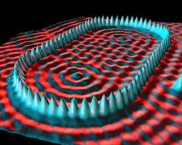
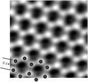
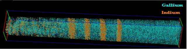
If you look on the internet for pictures of atoms, you will see images like this:
Or like this:
Or like this:
How do we “see” an atom?
Human vision and atomic scale
What we mean by “see” matters. For humans, seeing is based on visible light reaching our eyes and being interpreted by our brain. The naked eye has a resolution of roughly 100 microns. By comparison, interatomic spacing is on the order of a tenth of a nanometer. In that sense, we cannot see an individual atom with the unaided eye.
Diffraction limits of light
What about magnification? Even the best lenses and mirrors are limited by diffraction: roughly half a wavelength of light (≈200 nm). That is still around 1,000–2,000 atoms across, so conventional optical microscopes cannot resolve single atoms. If materials existed that could refract X-rays like glass refracts visible light, we might build an X-ray refractive microscope — but such materials do not exist for practical imaging.
What counts as “seeing” in microscopy
For this article I draw the line at visible-frequency passive optics (lenses and mirrors). If a microscope converts light to electrical signals, collects data for longer than the human eye, amplifies the signal digitally, or uses particles instead of light, then what we view is a reconstructed image displayed on a screen rather than direct vision by the eye.
Microscopy pronunciation
Note on pronunciation: “microscopy” is not pronounced like “microscope” with a final -y. The stress is on the “cro” syllable; it rhymes with “colonoscopy.” (Example: audio example)
Electron microscopy: TEM vs SEM
SEM overview
The electron microscopy images you commonly see online often come from scanning electron microscopes (SEMs). SEMs bounce a beam of electrons off a sample (often coated with metal) and produce surface images, but they do not typically achieve atomic resolution.
TEM overview
Transmission electron microscopes (TEMs) instead send electrons through a thin sample and detect electrons on the far side. A helpful analogy: if SEMs are like an ultrasound, TEMs are more like an X‑ray that reveals internal structure.
Interpreting TEM images
In a TEM image, bright regions usually correspond to areas where fewer electrons are blocked — that is, less material standing in the beam. When resolution is high, features that appear as bright dots are often the projected shadows of columns of atoms (a line-of-sight projection), not necessarily single atoms sitting isolated in a plane.
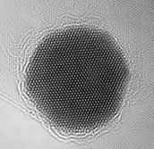
Modern TEM techniques can image single-layer materials such as graphene and directly reveal the hexagonal lattice of carbon atoms.
Atomic Force Microscopy (AFM)
How AFM works
An atomic force microscope (AFM) is a scanning probe instrument, not an electron microscope. It uses a small cantilever with a very sharp tip (often with an apex on the scale of a few atoms) that is rastered across a sample surface. A laser beam reflected off the cantilever detects deflections, and those deflections are recorded.
AFM modes
There are two common AFM modes:
- Tapping mode: the cantilever vibrates at its resonance frequency; interactions with the sample change that oscillation and the change is measured.
- Contact/constant-height mode: the tip is kept at a fixed height and measured deflections map the topography.
Tip sharpness and resolution
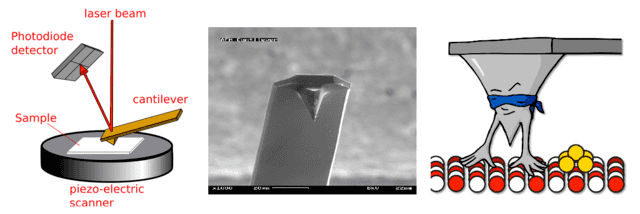
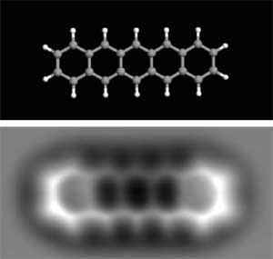
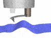
The AFM’s lateral resolution depends on tip sharpness. With a tip that ends in a single atom, AFM can achieve true atomic resolution by mapping surface height or force at each point. The tip scans line-by-line; on atomically flat surfaces each scan line looks like a repeating zig-zag pattern, and the assembled lines produce a 2D height map that can be rendered in 3D.
The organic-molecule image shown near the article start was created using AFM. Producing such images requires a very sharp tip and hours of slow, precise scanning.
Scanning Tunneling Microscopy (STM)
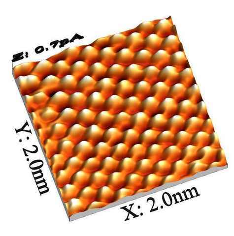
What STM measures
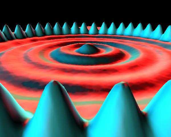
Scanning tunneling microscopy (STM) is another scanning probe technique. Instead of measuring forces, an STM applies a voltage between a conductive tip and the sample and measures the tunneling current. The tunneling probability reflects the local electronic density of states at the surface, so STM images often visualize electron wavefunctions rather than only atomic positions.
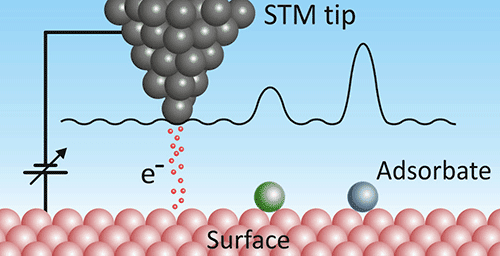
Visualization and rendering
STM images are commonly rendered in exaggerated 3D to make the atomic corrugation easier to see. The result can look like someone took a close-up “photograph” of an atom — but what STM actually maps is a combination of surface topography and electronic structure.
A boy and his atom: the world’s smallest movie
See the atomic-scale movie: https://www.youtube.com/watch?v=oSCX78-8-q0
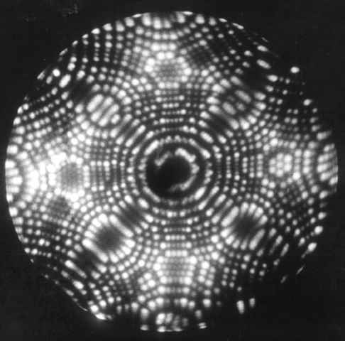
Field emission, field ion microscopy, and atom probe tomography
How FEM works
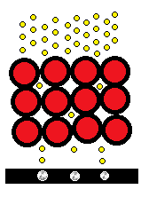
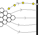
Field emission microscopy (FEM) is one of the older techniques with atomic resolution. A high voltage applied between a sharp tip (often tungsten) and a screen causes electrons to be emitted from the tip. The emitted electrons are deflected by the non-uniform electric field and strike a screen; tracing their trajectories back reveals the atomic layout on the tip surface.
Variants: FIM and APT
Variants include field ion microscopy (atoms on the tip are ionized and imaged) and atom probe tomography (APT), a destructive technique in which atoms are evaporated from the tip and their identities and original positions are reconstructed to build a 3D map.
3D atomic imaging
Atom Probe Tomography (APT)
Beyond 2D surface maps, some methods reconstruct 3D atomic positions. Atom Probe Tomography (APT) builds 3D maps by recording the order and position of atoms as they evaporate from a sharply shaped sample. It can also identify elements, but it is generally limited to small, needle-like specimens.
Tomographic TEM reconstructions
Recent work has fused TEM imaging with computed tomography (CT) style reconstructions: multiple 2D TEM projections taken at different angles are combined to produce a 3D map of atomic positions. One paper used this approach to reconstruct the locations of ≈27,000 atoms in a nanoparticle — a remarkable technical achievement.
Conclusion
Key takeaways
We cannot see atoms directly with our eyes or with classical optical microscopes. However, using electron- and probe-based techniques (TEM, STEM, AFM, STM, FEM, APT, and newer methods like electron ptychography and tomography) scientists can determine atomic positions and render those positions as images we can visually interpret.
These images are reconstructions or maps derived from measured signals (electron transmission, tunneling current, force, or emitted ions) rather than direct visible-light photographs. Still, they provide genuine, high-resolution insight into atomic arrangements and are continually improving.
Updates and related links
Update: Scientists have recently produced an even more detailed image of atomic structure: New image of atoms — New Scientist.
Related: Do we know what an electron looks like?
Ph.D. McGill University, 2015
My research is at the interface of biological physics and soft condensed matter. I am interested in using tools provided from biology to answer questions about the physics of soft materials. In the past I have investigated how DNA partitions itself into small spaces and how knots in DNA molecules move and untie. Moving forward, I will be investigating the physics of non-covalent chemical bonds using “DNA chainmail” and exploring non-equilibrium thermodynamics and fluid mechanics using protein gels.


Leave a Reply
Want to join the discussion?Feel free to contribute!